 ChipApex | Global Electronic Components Supplier

SEARCH
Search Product
Search Post
— IC芯片 | 连接器 | 传感器 | 被动器件 —
Search productSearch post
— IC芯片 | 连接器 | 传感器 | 被动器件 —
Consult the customer manager about the wholesale price.
consultation hotline:86-132-6715-2157
email:[email protected]
Contact the product manager for consultation. One-stop consultation is available.
Do you want a lower wholesale price? Please send us your inquiry and we will reply immediately.
ADS8401IBPFBT is listed in the Analog To Digital Converters (ADC) range at ChipApex. The manufacturer field lists Texas Instruments. Its product description is IC ADC 16BIT SAR 48TQFP. Review the specifications below when checking this part for your BOM.
The ADS8401IBPFBT is a 16-bit, 1.25 MSPS analog-to-digital converter (ADC) featuring a successive approximation register (SAR) architecture and a unipolar single-ended input range of 0 V to Vref. It integrates a 4.096-V internal reference with an onboard buffer. The device operates with a 5-V analog supply (+VA) and a wide digital supply (+VBD) ranging from 2.95 V to 5.25 V. Key electrical parameters include a maximum conversion time of 610 ns, a throughput rate of 1.25 MHz, and a typical power dissipation of 155 mW at full speed. It provides zero-latency data output via a high-speed parallel interface.
Verify the specific linearity grade required for the application. The 'I' suffix denotes ±6 LSB integral linearity, while the 'B' suffix denotes ±3.5 LSB. Ensure the ordering suffix matches the desired performance specification. Confirm package designator PFB corresponds to the 48-pin TQFP variant. Check RoHS compliance status as manufacturing processes may vary by production date.
Select the ADS8401IBPFBT when ±3.5 LSB integral linearity is required, as opposed to the ADS8401IPFBT which offers ±6 LSB. The device requires a 5-V analog supply and a digital supply between 2.95 V and 5.25 V. Ensure the system can accommodate the 48-lead TQFP package. Verify that the host microcontroller supports the required parallel interface timing and voltage levels for +VBD.
The ADS8401 belongs to Texas Instruments' family of micro-power sampling ADCs. It is characterized for operation over the industrial temperature range of –40°C to 85°C. The device is available in tape and reel packaging (suffix BT) with quantities of 250 units. It utilizes a capacitor-based SAR architecture for charge redistribution conversions.
Public confirmed substitute part numbers are not provided in the source documentation.
When using the internal reference, connect pin 2 (REFOUT) to pin 1 (REFIN) with a 0.1 µF decoupling capacitor and place a 1 µF storage capacitor between REFOUT and REFM (pins 47/48).
The BYTE pin allows reading the 16-bit result on an 8-bit bus. When low, DB15–DB8 output the most significant bits. When high, the same pins output the least significant bits (D7–D0), requiring two read cycles.
The analog supply (+VA) must be 5 V (range 4.75 V to 5.25 V). The digital supply (+VBD) ranges from 2.95 V to 5.25 V, with the constraint that +VBD ≥ +VA – 2.3 V.
Explore related parts through Data Acquisition, Integrated Circuits (ICs), all product categories, ChipApex homepage.
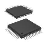 ADS8401IBPFBT
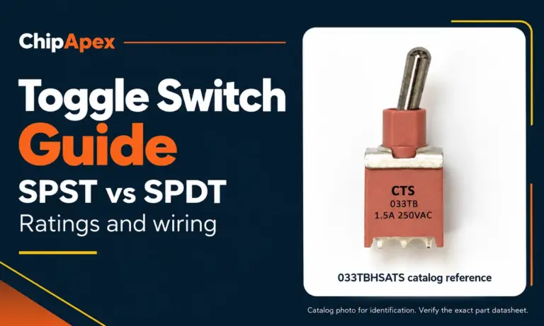
Compare SPST and SPDT toggle switches, understand AC/DC ratings, and follow wiring examples. Check contact action, mounting and parts in the ChipApex catalog.
Read More
Compare thermistors, RTDs, thermocouples and temperature ICs. Learn how range, accuracy, response, interfaces and mounting affect component selection.
Read More
Choose a DIP switch by contact type, coded positions, footprint and signal ratings. Check logic polarity, assembly conditions and PCB configuration behavior.
Read More
ADS8401IBPFBT is listed in the Analog To Digital Converters (ADC) range at ChipApex. The manufacturer field lists Texas Instruments. Its product description is IC…
Read More
ADS8401IBPFBT is listed in the Analog To Digital Converters (ADC) range at ChipApex. The manufacturer field lists Texas Instruments. Its product description is IC…
Read More
ADS8401IBPFBT is listed in the Analog To Digital Converters (ADC) range at ChipApex. The manufacturer field lists Texas Instruments. Its product description is IC…
Read More
Explore electronic component types, functions, packages and datasheets. Learn selection, replacement and BOM checks before ordering parts for your PCB.
Read MoreADS8401IBPFBT is listed in the Analog To Digital Converters (ADC) range at ChipApex. The manufacturer field lists Texas Instruments. Its product description is IC…
Read More
Choose an AC to DC converter by input range, output demand, isolation, efficiency and thermal derating. Compare architectures and check installation needs.
Read More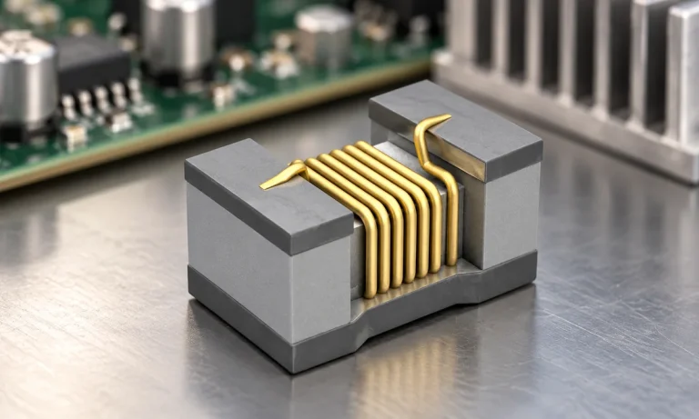
See when an inductor behaves linearly, how DC bias and saturation reduce inductance, and which current and temperature curves to check.
Read More
ADS8401IBPFBT is listed in the Analog To Digital Converters (ADC) range at ChipApex. The manufacturer field lists Texas Instruments. Its product description is IC…
Read More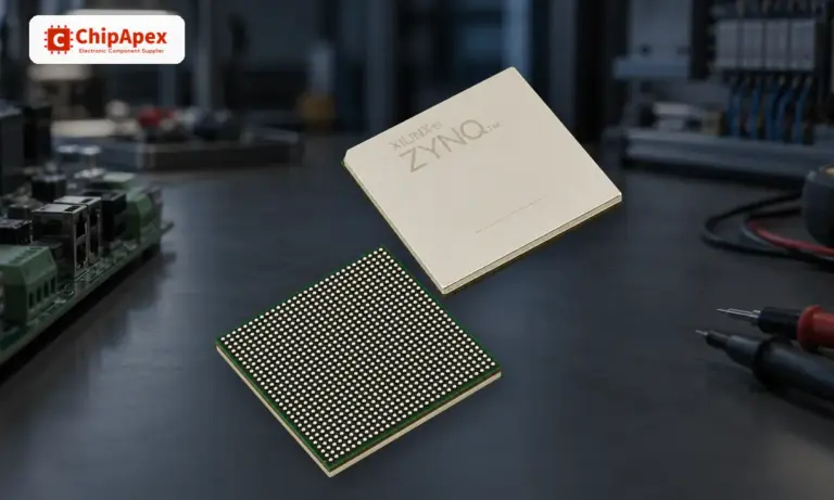
Learn what an integrated circuit is, how ICs work, the main types and the specs to check before choosing a part for your design…
Read More
The activity of extra discounts on wholesale prices is in full swing…
Please fill in your contact information and we will send you the latest wholesale price list.





