ChipApex | Global Electronic Components Supplier

SEARCH
Search Product
Search Post
— IC芯片 | 连接器 | 传感器 | 被动器件 —
Search productSearch post
— IC芯片 | 连接器 | 传感器 | 被动器件 —
Consult the customer manager about the wholesale price.
consultation hotline:86-132-6715-2157
email:[email protected]
Contact the product manager for consultation. One-stop consultation is available.
Do you want a lower wholesale price? Please send us your inquiry and we will reply immediately.
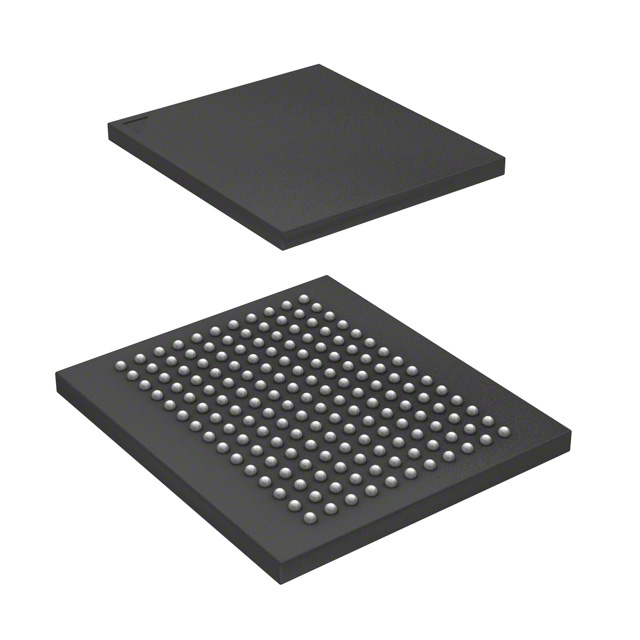
CY7C1513AV18-167BZC is listed in the Memory IC range at ChipApex. The manufacturer field lists Infineon Technologies. Its product description is IC SRAM 72MBIT PAR 165FBGA. Review the specifications below when checking this part for your BOM.
The CY7C1513AV18-167BZC is a 72-Mbit QDR-II SRAM with a 4M x 18 organization. It supports a maximum operating frequency of 167 MHz and operates within a core voltage range of 1.7 V to 1.9 V. The device utilizes a 165-ball FBGA package measuring 15 x 17 x 1.4 mm. Maximum operating current at this speed is 615 mA.
Verify component authenticity through authorized Infineon distributors or certified partners. Confirm RoHS compliance status as indicated by the suffix, noting that specific ordering variants may differ in lead-free characteristics. Validate package dimensions against the 165-ball FBGA specification before integration into PCB designs.
Select this model for applications requiring simultaneous read and write operations without bus turnaround delays. Ensure system design accommodates the 1.8V core voltage and 1.7V to 1.9V supply range. Verify that the host controller supports the required DDR interface timing and echo clock synchronization for optimal performance at 167 MHz.
This component belongs to the Cypress/Infineon QDR-II family of synchronous pipelined SRAMs. It shares architectural similarities with the CY7C1511AV18, CY7C1526AV18, and CY7C1515AV18, differing primarily in memory density and data width configurations while maintaining the same 165-ball FBGA footprint and interface protocols.
Direct pin-compatible substitutes include other members of the CY7C15xxAV18 series such as the CY7C1511AV18, CY7C1526AV18, and CY7C1515AV18, provided the system can accommodate differences in memory organization and data width.
The QDR-II architecture provides separate independent read and write ports, allowing concurrent transactions. Addresses are latched on alternating rising edges of the input clock, enabling simultaneous access without bus contention.
The DOFF pin controls the Delay Lock Loop (DLL). Connecting it to ground disables the DLL, causing the device to operate in QDR-I mode with one-cycle read latency and longer access times.
An external resistor (RQ) must be connected between the ZQ pin and ground. The value should be five times the intended line impedance, typically between 175 Ω and 350 Ω, to tune the output drivers.
Explore related parts through Memory, Integrated Circuits (ICs), all product categories, ChipApex homepage.
 CY7C1513AV18-167BZC

Learn what an IMU measures, how accelerometers and gyroscopes work together, why orientation estimates drift, and what to compare.
Read More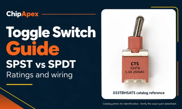
Compare SPST and SPDT toggle switches, understand AC/DC ratings, and follow wiring examples. Check contact action, mounting and parts in the ChipApex catalog.
Read More
CY7C1513AV18-167BZC is listed in the Memory IC range at ChipApex. The manufacturer field lists Infineon Technologies. Its product description is IC SRAM 72MBIT PAR…
Read More
Find out when a bare shock switch needs a pull resistor, when an MCU internal pull-up is enough, and why sensor modules and piezo…
Read More
CY7C1513AV18-167BZC is listed in the Memory IC range at ChipApex. The manufacturer field lists Infineon Technologies. Its product description is IC SRAM 72MBIT PAR…
Read More
Explore electronic component types, functions, packages and datasheets. Learn selection, replacement and BOM checks before ordering parts for your PCB.
Read More
CY7C1513AV18-167BZC is listed in the Memory IC range at ChipApex. The manufacturer field lists Infineon Technologies. Its product description is IC SRAM 72MBIT PAR…
Read More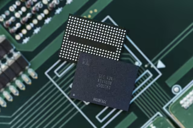
CY7C1513AV18-167BZC is listed in the Memory IC range at ChipApex. The manufacturer field lists Infineon Technologies. Its product description is IC SRAM 72MBIT PAR…
Read More
CY7C1513AV18-167BZC is listed in the Memory IC range at ChipApex. The manufacturer field lists Infineon Technologies. Its product description is IC SRAM 72MBIT PAR…
Read More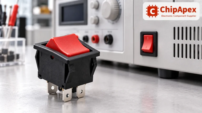
Choose a rocker switch by AC/DC ratings, contact arrangement, illumination, panel fit and sealing. Get practical checks for engineering and component sourcing.
Read More
CY7C1513AV18-167BZC is listed in the Memory IC range at ChipApex. The manufacturer field lists Infineon Technologies. Its product description is IC SRAM 72MBIT PAR…
Read More
CY7C1513AV18-167BZC is listed in the Memory IC range at ChipApex. The manufacturer field lists Infineon Technologies. Its product description is IC SRAM 72MBIT PAR…
Read More
The activity of extra discounts on wholesale prices is in full swing…
Please fill in your contact information and we will send you the latest wholesale price list.