 ChipApex | Global Electronic Components Supplier
DG408LEDN-T1-GE4
Search Product
Search Post
— IC芯片 | 连接器 | 传感器 | 被动器件 —
Search productSearch post
— IC芯片 | 连接器 | 传感器 | 被动器件 —
Consult the customer manager about the wholesale price.
consultation hotline:86-132-6715-2157
email:[email protected]
Contact the product manager for consultation. One-stop consultation is available.
Do you want a lower wholesale price? Please send us your inquiry and we will reply immediately.
The DG408LEDN-T1-GE4 is an 8-channel single-ended analog multiplexer from the Vishay Siliconix DG408LE series, housed in a 16-pin QFN (3 mm x 3 mm) package. It operates on single supplies of 3 V to 16 V or dual supplies of ±3 V to ±8 V. The device features a typical on-resistance of 17 Ω and maximum leakage current of 1 nA. Key dynamic parameters include a maximum enable turn-on time of 72 ns and off-isolation of -99 dB at 100 kHz. It includes an internal regulator for low power consumption and TTL/CMOS compatible logic inputs.
Verify the specific ordering suffix against the manufacturer's official documentation to confirm package type and compliance status. The 'N' suffix indicates the QFN16 package, while 'T1' denotes tape and reel packaging. Confirm RoHS compliance details directly with the supplier or datasheet as required by project specifications.
Select this component when high channel count and low on-resistance are required in a compact surface-mount footprint. Ensure the application voltage stays within the 3 V to 16 V single supply or ±3 V to ±8 V dual supply limits. Consider the QFN package thermal characteristics and exposed pad connection requirements for proper heat dissipation.
This part belongs to the DG408LE family, which offers enhanced performance over standard DG408 devices. It provides lower on-resistance and improved leakage characteristics. The QFN16 package variant allows for smaller board space utilization compared to SOIC or TSSOP alternatives within the same functional family.
DG408LDY-T1-E3
The Enable (EN) pin allows the user to reset all switches to the off state, which is useful for stacking several devices.
All control inputs, including address and enable pins, are TTL compatible over the full specified operating temperature range.
The typical on-resistance (RDS(on)) is 17 Ω at +12 V / ±5 V / +5 V / +3 V supplies.
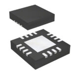 DG408LEDN-T1-GE4
The activity of extra discounts on wholesale prices is in full swing…
Please fill in your contact information and we will send you the latest wholesale price list.





