 ChipApex | Global Electronic Components Supplier
DG409DJ+
Search Product
Search Post
— IC芯片 | 连接器 | 传感器 | 被动器件 —
Search productSearch post
— IC芯片 | 连接器 | 传感器 | 被动器件 —
Consult the customer manager about the wholesale price.
consultation hotline:86-132-6715-2157
email:[email protected]
Contact the product manager for consultation. One-stop consultation is available.
Do you want a lower wholesale price? Please send us your inquiry and we will reply immediately.
The DG409DJ+ is a dual 4-channel CMOS analog multiplexer/demultiplexer manufactured by Analog Devices Inc./Maxim Integrated. It operates with single supplies from +5V to +30V or dual supplies from ±5V to ±20V. The device features a maximum on-resistance of 100Ω, guaranteed channel matching of 8Ω max, and flatness of 9Ω max. Key electrical parameters include a maximum charge injection of 15pC, input leakage current under 5nA at +85°C, and low power consumption of 1.25mW max. It provides ESD protection exceeding 2000V per MIL-STD-883 Method 3015.7 and functions within a temperature range of -40°C to +85°C in a 16-pin Plastic DIP package.
Verify the specific ordering suffix against official documentation to confirm the package type and temperature rating. The 'D' suffix indicates an extended industrial temperature range (-40°C to +85°C), while the 'J' suffix denotes a plastic DIP package. Ensure compatibility with existing board layouts as these devices are designed as direct pin-compatible replacements for legacy components.
Select this component when high channel matching and low on-resistance flatness are required for precision analog switching applications. The DG409DJ+ is suitable for designs needing rail-to-rail signal handling and robust ESD protection. Consider the supply voltage requirements, as switching times may increase significantly at lower supply voltages such as 5V.
The DG409DJ+ belongs to the DG408/DG409 family of improved CMOS analog multiplexers. This series represents a redesign of earlier industry-standard parts, offering enhanced performance metrics such as guaranteed channel matching and reduced charge injection. The device serves as a direct upgrade path for systems utilizing legacy DG408 or DG409 components without requiring schematic modifications.
DG409EUE+
The DG409DJ+ guarantees an on-resistance flatness of 9Ω maximum over the specified signal range.
Signals on inputs exceeding V+ or V- are clamped by internal diodes. For proper protection, it is recommended to sequence power supplies correctly or add external blocking diodes if sequencing is not possible.
Yes, the digital input controls are compatible with both TTL and CMOS logic standards.
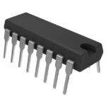 DG409DJ+
The activity of extra discounts on wholesale prices is in full swing…
Please fill in your contact information and we will send you the latest wholesale price list.





