 ChipApex | Global Electronic Components Supplier
DG409LDQ-E3
Search Product
Search Post
— IC芯片 | 连接器 | 传感器 | 被动器件 —
Search productSearch post
— IC芯片 | 连接器 | 传感器 | 被动器件 —
Consult the customer manager about the wholesale price.
consultation hotline:86-132-6715-2157
email:[email protected]
Contact the product manager for consultation. One-stop consultation is available.
Do you want a lower wholesale price? Please send us your inquiry and we will reply immediately.
The DG409LDQ-E3 is a dual 4-channel differential analog multiplexer manufactured by Vishay Siliconix. It operates on single supplies from 2.7 V to 12 V or dual supplies of ±3 V to ±6 V. The device connects one of four differential inputs to a common dual output using a 2-bit binary address (A0, A1). Key electrical parameters include a typical on-resistance of 17 Ω, enable turn-on time of 38 ns, and enable turn-off time of 18 ns. Maximum switch off leakage current is 1 nA at room temperature. The component utilizes BiCMOS technology for low power consumption and high accuracy.
Verify the specific suffix 'D' indicates the -40 °C to +85 °C operating range and 'Q' denotes the TSSOP-16 package. Confirm RoHS compliance status via the manufacturer's documentation as ordering suffixes may affect material categorization. Ensure the design supports the required voltage levels for the selected supply configuration.
Select this part when differential signal routing is required in space-constrained designs due to its compact TSSOP-16 footprint. Verify that the system voltage falls within the 2.7 V to 12 V single supply or ±3 V to ±6 V dual supply limits. Consider the 17 Ω typical on-resistance for signal loss calculations in precision applications.
This component belongs to the DG408L/DG409L series, which are low-voltage companion devices to the industry-standard DG408/DG409. The L-series offers improved performance characteristics including lower on-resistance, faster switching times, and reduced leakage compared to the original versions while maintaining pin compatibility.
DG409LDY-T1-E3
The analog signal range extends from V- to V+, allowing operation across the full supply voltage range.
It features guaranteed break-before-make switching action, which prevents momentary crosstalk between adjacent channels during transitions.
The device is compatible with TTL, CMOS, and Low Voltage (LV) logic families operating at 3 V.
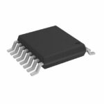 DG409LDQ-E3
The activity of extra discounts on wholesale prices is in full swing…
Please fill in your contact information and we will send you the latest wholesale price list.





