 ChipApex | Global Electronic Components Supplier

SEARCH
Search Product
Search Post
— IC芯片 | 连接器 | 传感器 | 被动器件 —
Search productSearch post
— IC芯片 | 连接器 | 传感器 | 被动器件 —
Consult the customer manager about the wholesale price.
consultation hotline:86-132-6715-2157
email:[email protected]
Contact the product manager for consultation. One-stop consultation is available.
Do you want a lower wholesale price? Please send us your inquiry and we will reply immediately.
FST3345QSCX is listed in the Signal Switches, Multiplexers, Decoders range at ChipApex. The manufacturer field lists onsemi. Its product description is IC BUS SWITCH 8 X 1:1 20QSOP. Review the specifications below when checking this part for your BOM.
The FST3345QSCX is an 8-bit bus switch manufactured by onsemi. It provides high-speed CMOS TTL-compatible bus switching with a low on-resistance of 4 Ω between two ports. The device operates within a power supply voltage range of 4.0 V to 5.5 V and supports an input/output voltage range of 0 V to 5.5 V. It features dual output enable inputs (OE and /OE) for flexible control, allowing the connection or disconnection of Port A from Port B. The component is housed in a 20-lead Thin Shrink Small Outline Package (TSSOP).
Verify the exact part number against current manufacturer databases, as legacy Fairchild Semiconductor orderable part numbers may have been updated to meet ON Semiconductor system requirements following integration. Confirm package dimensions and tape-and-reel specifications match your manufacturing equipment before finalizing procurement orders.
Select this component when designing circuits that require bidirectional data transfer between buses with minimal signal degradation. Ensure the operating voltage aligns with the specified 4.0 V to 5.5 V range. Verify that the 20-lead TSSOP package fits the available PCB footprint and that the thermal characteristics support the intended operating temperature range of -40°C to +85°C.
This device belongs to the FST series of bus switches, originally developed by Fairchild Semiconductor before its acquisition by ON Semiconductor. The series is designed for high-speed digital applications where low on-resistance and minimal propagation delay are critical for maintaining signal integrity across connected buses.
Check the official ON Semiconductor website for updated ordering information, as legacy Fairchild part numbers containing underscores may have been converted to dashes. Verify pinout compatibility if considering alternative bus switch ICs from other manufacturers.
The device is designed to exhibit zero bounce in flow-through mode, ensuring clean signal transitions during switching operations.
The typical quiescent supply current (ICC) is 3 µA when VIN is at VCC or GND and IOUT is 0.
Explore related parts through Logic, Integrated Circuits (ICs), all product categories, ChipApex homepage.
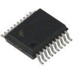 FST3345QSCX
Learn how rectifiers convert AC to DC, compare half-wave and bridge circuits, and select voltage, current, recovery and thermal ratings for your design.
Read More
Learn the relay definition, coil and contact operation, NO and NC forms, load ratings and suppression choices. Compare mechanical, reed and solid-state types.
Read More
FST3345QSCX is listed in the Signal Switches, Multiplexers, Decoders range at ChipApex. The manufacturer field lists onsemi. Its product description is IC BUS SWITCH…
Read More
FST3345QSCX is listed in the Signal Switches, Multiplexers, Decoders range at ChipApex. The manufacturer field lists onsemi. Its product description is IC BUS SWITCH…
Read More
FST3345QSCX is listed in the Signal Switches, Multiplexers, Decoders range at ChipApex. The manufacturer field lists onsemi. Its product description is IC BUS SWITCH…
Read More
Learn what an integrated circuit is, how ICs work, the main types and the specs to check before choosing a part for your design…
Read More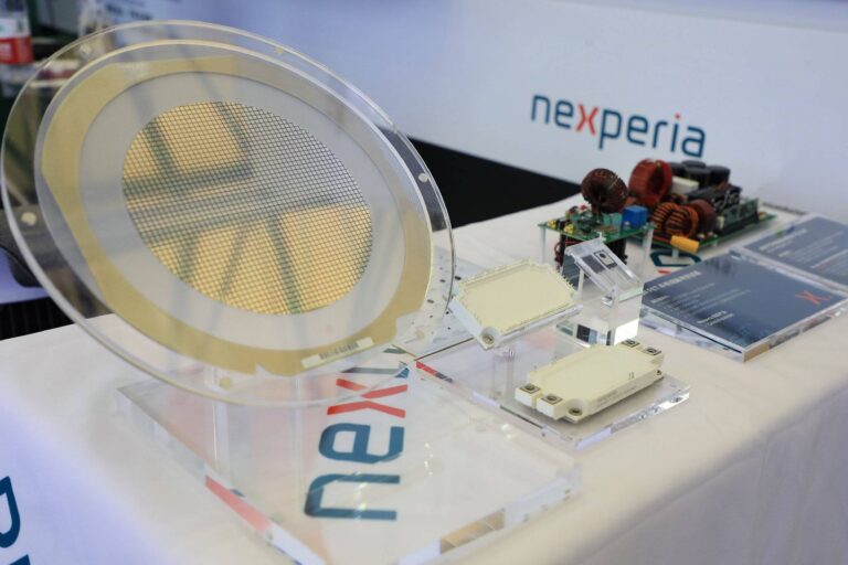
FST3345QSCX is listed in the Signal Switches, Multiplexers, Decoders range at ChipApex. The manufacturer field lists onsemi. Its product description is IC BUS SWITCH…
Read More
FST3345QSCX is listed in the Signal Switches, Multiplexers, Decoders range at ChipApex. The manufacturer field lists onsemi. Its product description is IC BUS SWITCH…
Read More
FST3345QSCX is listed in the Signal Switches, Multiplexers, Decoders range at ChipApex. The manufacturer field lists onsemi. Its product description is IC BUS SWITCH…
Read More
FST3345QSCX is listed in the Signal Switches, Multiplexers, Decoders range at ChipApex. The manufacturer field lists onsemi. Its product description is IC BUS SWITCH…
Read More
Learn how a diode conducts, how to identify anode and cathode, and when to choose rectifier, TVS, Zener or photodiode types for a circuit.
Read More
FST3345QSCX is listed in the Signal Switches, Multiplexers, Decoders range at ChipApex. The manufacturer field lists onsemi. Its product description is IC BUS SWITCH…
Read More
The activity of extra discounts on wholesale prices is in full swing…
Please fill in your contact information and we will send you the latest wholesale price list.







