 ChipApex | Global Electronic Components Supplier

SEARCH
Search Product
Search Post
— IC芯片 | 连接器 | 传感器 | 被动器件 —
Search productSearch post
— IC芯片 | 连接器 | 传感器 | 被动器件 —
Consult the customer manager about the wholesale price.
consultation hotline:86-132-6715-2157
email:[email protected]
Contact the product manager for consultation. One-stop consultation is available.
Do you want a lower wholesale price? Please send us your inquiry and we will reply immediately.
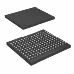
IDT71P72804S167BQ is listed in the Memory IC range at ChipApex. The manufacturer field lists Renesas Electronics Corporation. Its product description is IC SRAM 18MBIT PAR 165CABGA. Review the specifications below when checking this part for your BOM.
The IDT71P72804S167BQ is an 18Mb QDR II SRAM featuring independent, double-data-rate read and write data ports. It supports concurrent transactions with a burst of two words per access. The device utilizes a DDR multiplexed address bus and provides four word transfers per clock cycle for quad-data-rate performance. It operates on a 1.8V core voltage with scalable HSTL I/O interfaces ranging from 1.4V to 1.9V. The component is available in a 165-ball fBGA package.
Verify the specific speed grade and temperature range required for your application against the datasheet specifications. Confirm that the 165-ball fBGA package dimensions match your PCB footprint. Ensure proper termination resistors are used for the ZQ pin to maintain correct output impedance matching. Check for any RoHS compliance status updates as this component may have been discontinued or subject to product change notices.
Select this component when high throughput and low latency are critical requirements. The independent ports simplify system design by eliminating bidirectional buses. Consider the scalable I/O voltage range if interfacing with different logic levels. Ensure the system can support the required clock frequencies and power supply stability for DLL operation.
This part belongs to the QDR II SRAM family developed by Integrated Device Technology, now part of Renesas Electronics. These devices are designed for applications requiring maximum bandwidth and deterministic latency. The QDR technology offers significant performance advantages over standard SRAMs by allowing simultaneous read and write operations without bus contention.
IDT71P72804S167BQ
The QDR II architecture uses independent read and write ports, allowing simultaneous access. This eliminates the need for bidirectional buses and enables four word transfers per clock cycle, significantly increasing throughput compared to single data rate devices.
The ZQ pin is used for output impedance matching. An external resistor connected between ZQ and ground sets the drive strength of the output drivers, allowing the device to adapt to system transmission lines and reduce signal reflections.
Explore related parts through Memory, Integrated Circuits (ICs), all product categories, ChipApex homepage.
 IDT71P72804S167BQ

IDT71P72804S167BQ is listed in the Memory IC range at ChipApex. The manufacturer field lists Renesas Electronics Corporation. Its product description is IC SRAM 18MBIT…
Read More
Understand RF attenuator dB values, fixed and programmable types, impedance, power limits and noise tradeoffs before choosing parts for an RF signal path.
Read More
IDT71P72804S167BQ is listed in the Memory IC range at ChipApex. The manufacturer field lists Renesas Electronics Corporation. Its product description is IC SRAM 18MBIT…
Read More
IDT71P72804S167BQ is listed in the Memory IC range at ChipApex. The manufacturer field lists Renesas Electronics Corporation. Its product description is IC SRAM 18MBIT…
Read More
Understand how oscillators generate timing signals, how they differ from crystals, and which frequency, output and stability specs matter when choosing one.
Read More
IDT71P72804S167BQ is listed in the Memory IC range at ChipApex. The manufacturer field lists Renesas Electronics Corporation. Its product description is IC SRAM 18MBIT…
Read More
Select MOV varistors by continuous voltage, clamping behavior, surge waveform and repetition. Check thermal disconnection, fuse coordination and replacements.
Read More
IDT71P72804S167BQ is listed in the Memory IC range at ChipApex. The manufacturer field lists Renesas Electronics Corporation. Its product description is IC SRAM 18MBIT…
Read MoreIDT71P72804S167BQ is listed in the Memory IC range at ChipApex. The manufacturer field lists Renesas Electronics Corporation. Its product description is IC SRAM 18MBIT…
Read More
Compare thermistors, RTDs, thermocouples and temperature ICs. Learn how range, accuracy, response, interfaces and mounting affect component selection.
Read More
IDT71P72804S167BQ is listed in the Memory IC range at ChipApex. The manufacturer field lists Renesas Electronics Corporation. Its product description is IC SRAM 18MBIT…
Read More
Compare Pt100 and Pt1000 RTDs, two-, three- and four-wire connections, excitation and self-heating. Build an error budget from element to reported temperature.
Read More
The activity of extra discounts on wholesale prices is in full swing…
Please fill in your contact information and we will send you the latest wholesale price list.





