 ChipApex | Global Electronic Components Supplier

SEARCH
Search Product
Search Post
— IC芯片 | 连接器 | 传感器 | 被动器件 —
Search productSearch post
— IC芯片 | 连接器 | 传感器 | 被动器件 —
Consult the customer manager about the wholesale price.
consultation hotline:86-132-6715-2157
email:[email protected]
Contact the product manager for consultation. One-stop consultation is available.
Do you want a lower wholesale price? Please send us your inquiry and we will reply immediately.
LFE2-50E-7FN484C is listed in the Field Programmable Gate Array range at ChipApex. The manufacturer field lists Lattice Semiconductor Corporation. Its product description is IC FPGA 339 I/O 484FBGA. Review the specifications below when checking this part for your BOM.
The LFE2-50E-7FN484C is a Field Programmable Gate Array (FPGA) from the Lattice ECP2 family, manufactured by Lattice Semiconductor Corporation. It features 34,000 Adaptive Logic Modules (ALMs), 1.01 Mbit of embedded memory, and supports up to 500 I/O pins. The device operates within a supply voltage range of 1.14 V to 1.26 V and functions at data rates up to 750 Mb/s. It is housed in a 484-pin FineLine BGA package with dimensions of 23x23 mm, designed for surface mount technology applications.
Verify the specific suffix '7' indicates the -7 speed grade when sourcing replacements. Confirm the FN484C designation matches the required 484-pin FineLine BGA package type. Ensure the manufacturer is identified as Lattice Semiconductor Corporation to avoid confusion with legacy EC family parts. Cross-reference the RoHS compliance status if environmental regulations apply to your assembly process.
Select this component when a balance between moderate logic density and high I/O count is required. The ECP2 architecture offers lower power consumption compared to older FPGA families while maintaining competitive performance. Consider the 484-pin footprint constraints during PCB layout planning. Evaluate the 1.2V operating voltage against available power rails in the target system design.
This part belongs to the Lattice ECP2 family, which succeeded the original EC series. It provides enhanced logic resources and memory capacity over previous generations like the LFEC15E. The ECP2 series is known for its cost-effective solution for mid-range FPGA applications requiring significant I/O connectivity.
LFE2-50E-5FN484C: Same package and logic density but slower speed grade (-5 vs -7). LFE2-35E-7FN484C: Lower logic density (32k ALMs) but same speed and package.
Explore related parts through Embedded, Integrated Circuits (ICs), all product categories, ChipApex homepage.
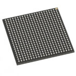 LFE2-50E-7FN484C

Choose a DIP switch by contact type, coded positions, footprint and signal ratings. Check logic polarity, assembly conditions and PCB configuration behavior.
Read More
LFE2-50E-7FN484C is listed in the Field Programmable Gate Array range at ChipApex. The manufacturer field lists Lattice Semiconductor Corporation. Its product description is IC…
Read More
Choose logic inverter ICs by thresholds, supply, output drive and delay. Compare standard and Schmitt-trigger inputs, power sequencing and replacement checks.
Read More
Learn what an IMU measures, how accelerometers and gyroscopes work together, why orientation estimates drift, and what to compare.
Read More
Learn how a diode conducts, how to identify anode and cathode, and when to choose rectifier, TVS, Zener or photodiode types for a circuit.
Read More
Compare RC, crystal and MEMS oscillator circuits. Check ppm, jitter, load capacitance, startup margin and output compatibility before choosing a clock source.
Read More
LFE2-50E-7FN484C is listed in the Field Programmable Gate Array range at ChipApex. The manufacturer field lists Lattice Semiconductor Corporation. Its product description is IC…
Read More
LFE2-50E-7FN484C is listed in the Field Programmable Gate Array range at ChipApex. The manufacturer field lists Lattice Semiconductor Corporation. Its product description is IC…
Read More
LFE2-50E-7FN484C is listed in the Field Programmable Gate Array range at ChipApex. The manufacturer field lists Lattice Semiconductor Corporation. Its product description is IC…
Read More
LFE2-50E-7FN484C is listed in the Field Programmable Gate Array range at ChipApex. The manufacturer field lists Lattice Semiconductor Corporation. Its product description is IC…
Read More
LFE2-50E-7FN484C is listed in the Field Programmable Gate Array range at ChipApex. The manufacturer field lists Lattice Semiconductor Corporation. Its product description is IC…
Read More
LFE2-50E-7FN484C is listed in the Field Programmable Gate Array range at ChipApex. The manufacturer field lists Lattice Semiconductor Corporation. Its product description is IC…
Read More
The activity of extra discounts on wholesale prices is in full swing…
Please fill in your contact information and we will send you the latest wholesale price list.





