ChipApex | Global Electronic Components Supplier

SEARCH
Search Product
Search Post
— IC芯片 | 连接器 | 传感器 | 被动器件 —
Search productSearch post
— IC芯片 | 连接器 | 传感器 | 被动器件 —
Consult the customer manager about the wholesale price.
consultation hotline:86-132-6715-2157
email:[email protected]
Contact the product manager for consultation. One-stop consultation is available.
Do you want a lower wholesale price? Please send us your inquiry and we will reply immediately.
LM358DR2G is listed in the Instrumentation, Op Amps, Buffer Amps range at ChipApex. The manufacturer field lists onsemi. Its product description is IC OPAMP GP 2 CIRCUIT 8SOIC. Review the specifications below when checking this part for your BOM.
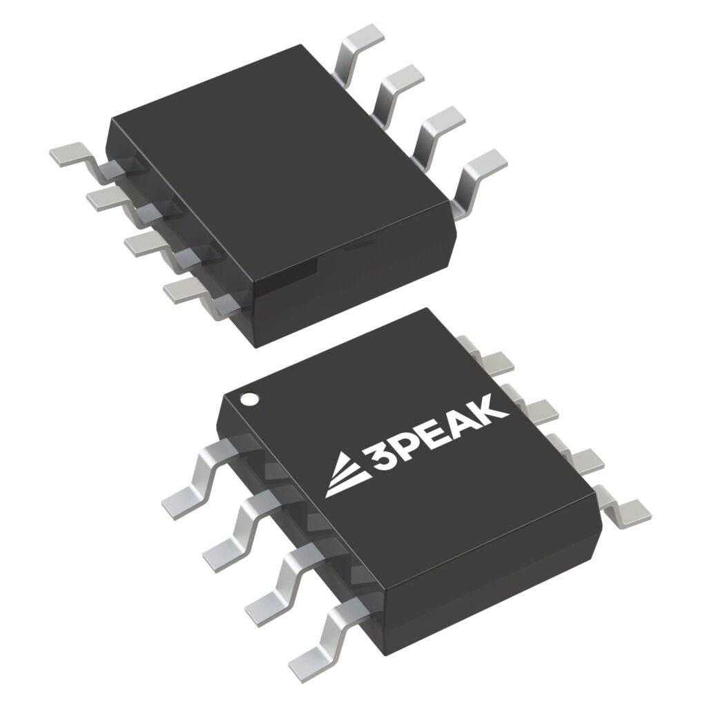
The LM358DR2G is a dual operational amplifier from onsemi, housed in an SOIC-8 package. It operates on single or split supplies ranging from 3.0 V to 32 V. Key electrical parameters include a typical input offset voltage of 7 mV and a maximum input bias current of 150 nA at 25°C. The device features internally compensated amplifiers with short-circuit protected outputs. It supports continuous output short circuits to ground and withstands ±32 V differential input voltages without damage.
Verify the specific suffix DR2G corresponds to the SOIC-8 tape and reel packaging configuration. Confirm that the operating temperature range aligns with the standard commercial grade specifications (0°C to +70°C) rather than automotive or extended variants. Ensure compliance with RoHS requirements if applicable to the target assembly process.
Select this component when single-supply operation down to 3 V is required. The low quiescent current makes it suitable for battery-powered systems. Consider the input offset voltage and bias current limits for precision applications. Verify that the load conditions do not exceed the specified output source and sink currents.
This device belongs to the LM358 series, which is equivalent to one-half of an LM324 quad operational amplifier. The series utilizes circuit designs perfected for quad amplifiers to provide low power drain and wide supply voltage ranges. It serves as a general-purpose dual op amp solution for various analog signal processing tasks.
LM358DR
No, the input common mode voltage or either input signal voltage should not be allowed to go negative by more than 0.3 V.
The device can withstand a differential input voltage of ±32 V without damage, independent of the magnitude of the supply voltage.
Explore related parts through Amplifiers, Linear, Integrated Circuits (ICs), all product categories.
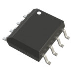 LM358DR2G

Choose a DIP switch by contact type, coded positions, footprint and signal ratings. Check logic polarity, assembly conditions and PCB configuration behavior.
Read More
LM358DR2G is listed in the Instrumentation, Op Amps, Buffer Amps range at ChipApex. The manufacturer field lists onsemi. Its product description is IC OPAMP…
Read More
LM358DR2G is listed in the Instrumentation, Op Amps, Buffer Amps range at ChipApex. The manufacturer field lists onsemi. Its product description is IC OPAMP…
Read More
LM358DR2G is listed in the Instrumentation, Op Amps, Buffer Amps range at ChipApex. The manufacturer field lists onsemi. Its product description is IC OPAMP…
Read More
LM358DR2G is listed in the Instrumentation, Op Amps, Buffer Amps range at ChipApex. The manufacturer field lists onsemi. Its product description is IC OPAMP…
Read More
LM358DR2G is listed in the Instrumentation, Op Amps, Buffer Amps range at ChipApex. The manufacturer field lists onsemi. Its product description is IC OPAMP…
Read More
LM358DR2G is listed in the Instrumentation, Op Amps, Buffer Amps range at ChipApex. The manufacturer field lists onsemi. Its product description is IC OPAMP…
Read More
LM358DR2G is listed in the Instrumentation, Op Amps, Buffer Amps range at ChipApex. The manufacturer field lists onsemi. Its product description is IC OPAMP…
Read More
LM358DR2G is listed in the Instrumentation, Op Amps, Buffer Amps range at ChipApex. The manufacturer field lists onsemi. Its product description is IC OPAMP…
Read More
Compare RC, crystal and MEMS oscillator circuits. Check ppm, jitter, load capacitance, startup margin and output compatibility before choosing a clock source.
Read More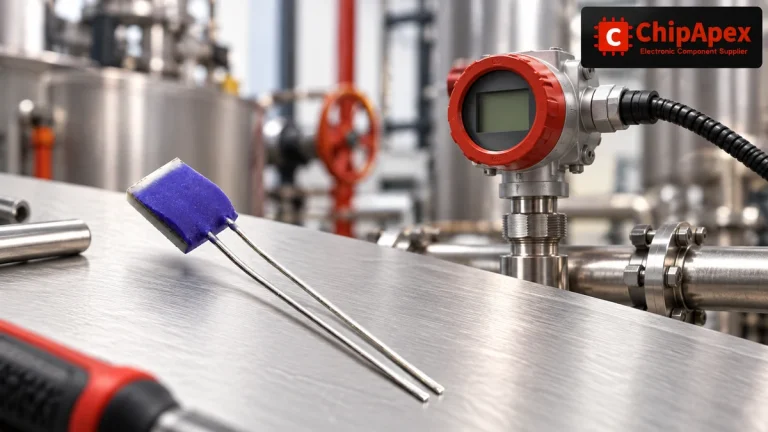
Compare Pt100 and Pt1000 RTDs, two-, three- and four-wire connections, excitation and self-heating. Build an error budget from element to reported temperature.
Read More
LM358DR2G is listed in the Instrumentation, Op Amps, Buffer Amps range at ChipApex. The manufacturer field lists onsemi. Its product description is IC OPAMP…
Read More
The activity of extra discounts on wholesale prices is in full swing…
Please fill in your contact information and we will send you the latest wholesale price list.