 ChipApex | Global Electronic Components Supplier

SEARCH
Search Product
Search Post
— IC芯片 | 连接器 | 传感器 | 被动器件 —
Search productSearch post
— IC芯片 | 连接器 | 传感器 | 被动器件 —
Consult the customer manager about the wholesale price.
consultation hotline:86-132-6715-2157
email:[email protected]
Contact the product manager for consultation. One-stop consultation is available.
Do you want a lower wholesale price? Please send us your inquiry and we will reply immediately.
MC74LVX257DTR2 is listed in the Signal Switches, Multiplexers, Decoders range at ChipApex. The manufacturer field lists onsemi. Its product description is IC MULTIPLEXER 4 X 2:1 16TSSOP. Review the specifications below when checking this part for your BOM.
The MC74LVX257DTR2 is a quad 2-channel multiplexer with 3-state outputs fabricated using advanced high-speed silicon gate CMOS technology. It features four independent 2-input digital multiplexers sharing common select (S) and output enable (OE) inputs. The device operates within a voltage range of 2.0 V to 3.6 V, with input voltages tolerating up to 7.0 V for interfacing with 5.0 V systems. Propagation delay is typically 4.5 ns at 3.3 V. It includes power-down protection on inputs and balanced propagation delays.
Verify the specific package suffix matches the required form factor, as the MC74LVX257 series is available in SOIC-16, TSSOP-16, and SOEIAJ-16 configurations. Confirm RoHS compliance status if lead-free materials are mandatory for the assembly process. Ensure the ordering quantity aligns with the manufacturer's standard shipping units for the selected tape and reel or tube packaging option.
Select this component when designing circuits requiring multiple independent data paths with low power consumption. The LVX series is suitable for applications needing operation down to 2.0 V. Verify that the 7.0 V input tolerance meets the requirements for interfacing with higher voltage logic levels without additional level shifting components.
This part belongs to the MC74LVX family of high-speed CMOS logic devices manufactured by onsemi. The LVX series is designed for low-voltage applications while maintaining compatibility with standard logic families. The MC74LVX257 specifically addresses multiplexing needs in compact surface-mount designs.
MC74LVX257DTG
When the Output Enable (OE) pin is held High, the selection of data is inhibited, and all outputs enter a high-impedance state.
The inputs can tolerate voltages up to 7.0 V, allowing safe interfacing with 5.0 V systems even when the device is powered at lower voltages.
Explore related parts through Logic, Integrated Circuits (ICs), all product categories, ChipApex homepage.
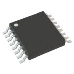 MC74LVX257DTR2
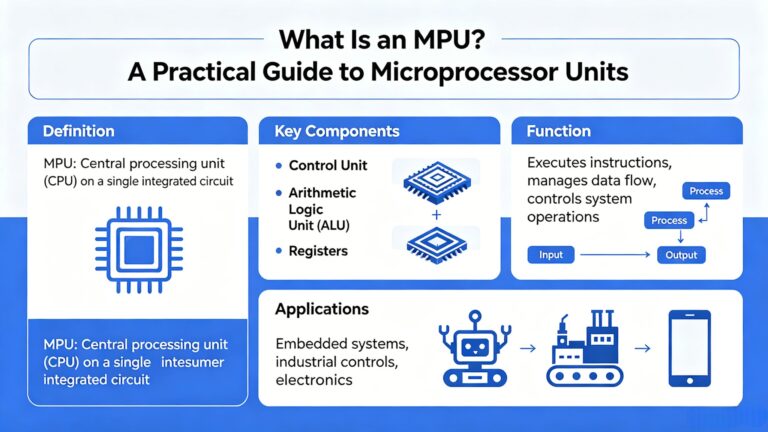
MC74LVX257DTR2 is listed in the Signal Switches, Multiplexers, Decoders range at ChipApex. The manufacturer field lists onsemi. Its product description is IC MULTIPLEXER 4…
Read More
MC74LVX257DTR2 is listed in the Signal Switches, Multiplexers, Decoders range at ChipApex. The manufacturer field lists onsemi. Its product description is IC MULTIPLEXER 4…
Read More
MC74LVX257DTR2 is listed in the Signal Switches, Multiplexers, Decoders range at ChipApex. The manufacturer field lists onsemi. Its product description is IC MULTIPLEXER 4…
Read More
MC74LVX257DTR2 is listed in the Signal Switches, Multiplexers, Decoders range at ChipApex. The manufacturer field lists onsemi. Its product description is IC MULTIPLEXER 4…
Read More
Learn how a JFET works and how to compare bias, leakage, noise and pinout. Review practical selection questions for high-impedance analog circuits.
Read More
Choose LED drivers by current, string voltage, dimming and thermal limits. Understand constant-current operation and the checks needed for your load.
Read More
MC74LVX257DTR2 is listed in the Signal Switches, Multiplexers, Decoders range at ChipApex. The manufacturer field lists onsemi. Its product description is IC MULTIPLEXER 4…
Read More
MC74LVX257DTR2 is listed in the Signal Switches, Multiplexers, Decoders range at ChipApex. The manufacturer field lists onsemi. Its product description is IC MULTIPLEXER 4…
Read More
Understand how a comparator switches at a voltage threshold, why hysteresis prevents chatter, and which output and input specs matter.
Read More
MC74LVX257DTR2 is listed in the Signal Switches, Multiplexers, Decoders range at ChipApex. The manufacturer field lists onsemi. Its product description is IC MULTIPLEXER 4…
Read More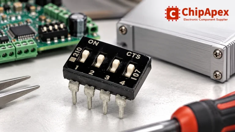
Choose a DIP switch by contact type, coded positions, footprint and signal ratings. Check logic polarity, assembly conditions and PCB configuration behavior.
Read More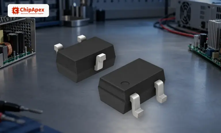
Learn how a diode conducts, how to identify anode and cathode, and when to choose rectifier, TVS, Zener or photodiode types for a circuit.
Read More
The activity of extra discounts on wholesale prices is in full swing…
Please fill in your contact information and we will send you the latest wholesale price list.





