 ChipApex | Global Electronic Components Supplier

SEARCH
Search Product
Search Post
— IC芯片 | 连接器 | 传感器 | 被动器件 —
Search productSearch post
— IC芯片 | 连接器 | 传感器 | 被动器件 —
Consult the customer manager about the wholesale price.
consultation hotline:86-132-6715-2157
email:[email protected]
Contact the product manager for consultation. One-stop consultation is available.
Do you want a lower wholesale price? Please send us your inquiry and we will reply immediately.
NB3V8312CMNG is listed in the Clock Buffers, Drivers range at ChipApex. The manufacturer field lists onsemi. Its product description is IC CLK BUFFER 1:12 250MHZ 32QFN. Review the specifications below when checking this part for your BOM.
The NB3V8312CMNG is a high-performance, low-skew LVCMOS fanout buffer manufactured by onsemi. It distributes one single-ended LVCMOS or LVTTL clock input to twelve LVCMOS outputs with a maximum operating frequency of 250 MHz. The device features synchronous clock enable and output enable controls, allowing outputs to be tri-stated or held low. It supports dual supply configurations where the core voltage (VDD) can be 3.3 V, 2.5 V, or 1.8 V, while the output supply (VDDO) operates at the same or lower voltage, provided VDD ≥ VDDO. This architecture enables lower power consumption and output-level compatibility. The component is housed in a 32-pin QFN package.
Verify the specific ordering suffix to confirm the package type and shipping quantity. The CMNG suffix indicates a QFN32 package supplied in tubes. Ensure that the required lead time and packaging specifications align with production schedules. Confirm compliance with RoHS directives and check for any recent product change notices that may affect availability or specifications before finalizing procurement orders.
Select this component when a single clock source must drive multiple loads with minimal skew. The dual-supply capability allows optimization of power dissipation by lowering the output voltage relative to the core. Ensure the input signal meets the specified LVCMOS or LVTTL amplitude requirements. Verify that the thermal resistance characteristics of the QFN32 package are adequate for the intended ambient temperature and airflow conditions.
This part belongs to the NB3V8312C family of ultra-low jitter fanout buffers. The family includes variants with different packages, such as the LQFP-32 option. These devices are designed for high-speed digital systems requiring precise clock distribution. The NB3V8312C series addresses the need for low phase noise and controlled propagation delay in complex electronic architectures.
Direct substitutes within the same family include the NB3V8312CFAG and NB3V8312CFAR2G, which utilize the LQFP-32 package instead of the QFN32 form factor. When replacing, ensure the pinout compatibility between the QFN and LQFP packages is managed through PCB design adjustments if necessary.
Explore related parts through Clock/Timing, Integrated Circuits (ICs), all product categories, ChipApex homepage.
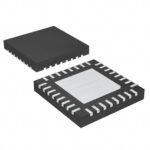 NB3V8312CMNG
See how a MEMS gyroscope measures angular rate, why its angle estimate drifts, and which range, noise, interface and temperature specs to compare.
Read More
NB3V8312CMNG is listed in the Clock Buffers, Drivers range at ChipApex. The manufacturer field lists onsemi. Its product description is IC CLK BUFFER 1:12…
Read More
NB3V8312CMNG is listed in the Clock Buffers, Drivers range at ChipApex. The manufacturer field lists onsemi. Its product description is IC CLK BUFFER 1:12…
Read More
Learn why PTC resistance rises with temperature, how it differs from NTC, and which ratings matter for sensing and protection.
Read More
NB3V8312CMNG is listed in the Clock Buffers, Drivers range at ChipApex. The manufacturer field lists onsemi. Its product description is IC CLK BUFFER 1:12…
Read More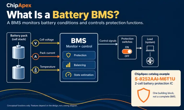
Learn what a battery BMS does, how protection differs from charging, and which pack specifications to check when sourcing BMS components through ChipApex.
Read More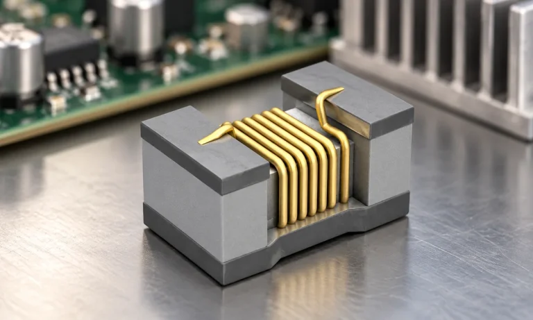
See when an inductor behaves linearly, how DC bias and saturation reduce inductance, and which current and temperature curves to check.
Read More
NB3V8312CMNG is listed in the Clock Buffers, Drivers range at ChipApex. The manufacturer field lists onsemi. Its product description is IC CLK BUFFER 1:12…
Read More
NB3V8312CMNG is listed in the Clock Buffers, Drivers range at ChipApex. The manufacturer field lists onsemi. Its product description is IC CLK BUFFER 1:12…
Read More
NB3V8312CMNG is listed in the Clock Buffers, Drivers range at ChipApex. The manufacturer field lists onsemi. Its product description is IC CLK BUFFER 1:12…
Read More
NB3V8312CMNG is listed in the Clock Buffers, Drivers range at ChipApex. The manufacturer field lists onsemi. Its product description is IC CLK BUFFER 1:12…
Read More
Choose logic inverter ICs by thresholds, supply, output drive and delay. Compare standard and Schmitt-trigger inputs, power sequencing and replacement checks.
Read More
The activity of extra discounts on wholesale prices is in full swing…
Please fill in your contact information and we will send you the latest wholesale price list.





