 ChipApex | Global Electronic Components Supplier

SEARCH
Search Product
Search Post
— IC芯片 | 连接器 | 传感器 | 被动器件 —
Search productSearch post
— IC芯片 | 连接器 | 传感器 | 被动器件 —
Consult the customer manager about the wholesale price.
consultation hotline:86-132-6715-2157
email:[email protected]
Contact the product manager for consultation. One-stop consultation is available.
Do you want a lower wholesale price? Please send us your inquiry and we will reply immediately.
NLX1G125FCT1G is listed in the Buffers, Drivers, Receivers, Transceivers range at ChipApex. The manufacturer field lists onsemi. Its product description is IC BUF NON-INVERT 5.5V 5FLIPCHIP. Review the specifications below when checking this part for your BOM.
The NLX1G125FCT1G is a non-inverting 3-state buffer manufactured by onsemi. It operates within a supply voltage range of 1.65 V to 5.5 V and features overvoltage tolerant input pins capable of withstanding up to 7.0 V regardless of the supply voltage. The device provides balanced propagation delays, typically 2.7 ns at 5.0 V, and offers 24 mA balanced output source and sink capability. It is designed for low power dissipation and is housed in an ultra-small 5-pin flip-chip package.
Verify that the component matches the specific 5-pin flip-chip package configuration required for your PCB layout. Confirm that the operating voltage range aligns with your system's power supply specifications. Ensure proper handling procedures are followed due to the small form factor. Check for any specific tape and reel requirements if automated assembly is planned.
Select this component when a compact, high-speed buffer with overvoltage tolerance is needed. Consider its low power consumption for battery-operated applications. Evaluate the 24 mA drive strength against load requirements. Verify compatibility with existing logic families and voltage levels in the target design.
This part belongs to onsemi's advanced high-speed CMOS logic family. It is designed for modern portable electronics requiring small footprints and low power consumption. The device complements other logic components in systems needing reliable signal buffering and isolation.
Check for direct pin-compatible alternatives from onsemi or other manufacturers offering similar electrical characteristics and package dimensions. Verify that any substitute maintains the same overvoltage tolerance and speed performance.
The input pins are overvoltage tolerant and can withstand voltages up to 7.0 V, regardless of the supply voltage level.
Yes, the typical propagation delay is 2.7 ns when operating at a supply voltage of 5.0 V.
Explore related parts through Logic, Integrated Circuits (ICs), all product categories, ChipApex homepage.
 NLX1G125FCT1G

NLX1G125FCT1G is listed in the Buffers, Drivers, Receivers, Transceivers range at ChipApex. The manufacturer field lists onsemi. Its product description is IC BUF NON-INVERT…
Read More
NLX1G125FCT1G is listed in the Buffers, Drivers, Receivers, Transceivers range at ChipApex. The manufacturer field lists onsemi. Its product description is IC BUF NON-INVERT…
Read More
NLX1G125FCT1G is listed in the Buffers, Drivers, Receivers, Transceivers range at ChipApex. The manufacturer field lists onsemi. Its product description is IC BUF NON-INVERT…
Read More
NLX1G125FCT1G is listed in the Buffers, Drivers, Receivers, Transceivers range at ChipApex. The manufacturer field lists onsemi. Its product description is IC BUF NON-INVERT…
Read More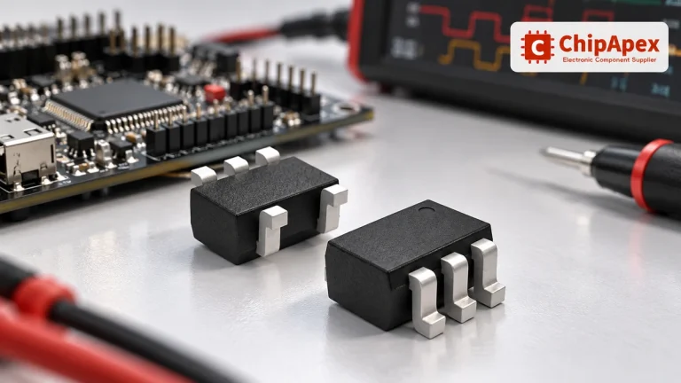
Choose logic inverter ICs by thresholds, supply, output drive and delay. Compare standard and Schmitt-trigger inputs, power sequencing and replacement checks.
Read More
Select a bridge rectifier by reverse voltage, capacitor charging current, startup surge and cooling. Work through a stated DC voltage and ripple example.
Read More
Learn what an integrated circuit is, how ICs work, the main types and the specs to check before choosing a part for your design…
Read More
Learn how rectifiers convert AC to DC, compare half-wave and bridge circuits, and select voltage, current, recovery and thermal ratings for your design.
Read More
NLX1G125FCT1G is listed in the Buffers, Drivers, Receivers, Transceivers range at ChipApex. The manufacturer field lists onsemi. Its product description is IC BUF NON-INVERT…
Read More
NLX1G125FCT1G is listed in the Buffers, Drivers, Receivers, Transceivers range at ChipApex. The manufacturer field lists onsemi. Its product description is IC BUF NON-INVERT…
Read More
NLX1G125FCT1G is listed in the Buffers, Drivers, Receivers, Transceivers range at ChipApex. The manufacturer field lists onsemi. Its product description is IC BUF NON-INVERT…
Read More
NLX1G125FCT1G is listed in the Buffers, Drivers, Receivers, Transceivers range at ChipApex. The manufacturer field lists onsemi. Its product description is IC BUF NON-INVERT…
Read More
The activity of extra discounts on wholesale prices is in full swing…
Please fill in your contact information and we will send you the latest wholesale price list.





