ChipApex | Global Electronic Components Supplier

SEARCH
Search Product
Search Post
— IC芯片 | 连接器 | 传感器 | 被动器件 —
Search productSearch post
— IC芯片 | 连接器 | 传感器 | 被动器件 —
Consult the customer manager about the wholesale price.
consultation hotline:86-132-6715-2157
email:[email protected]
Contact the product manager for consultation. One-stop consultation is available.
Do you want a lower wholesale price? Please send us your inquiry and we will reply immediately.
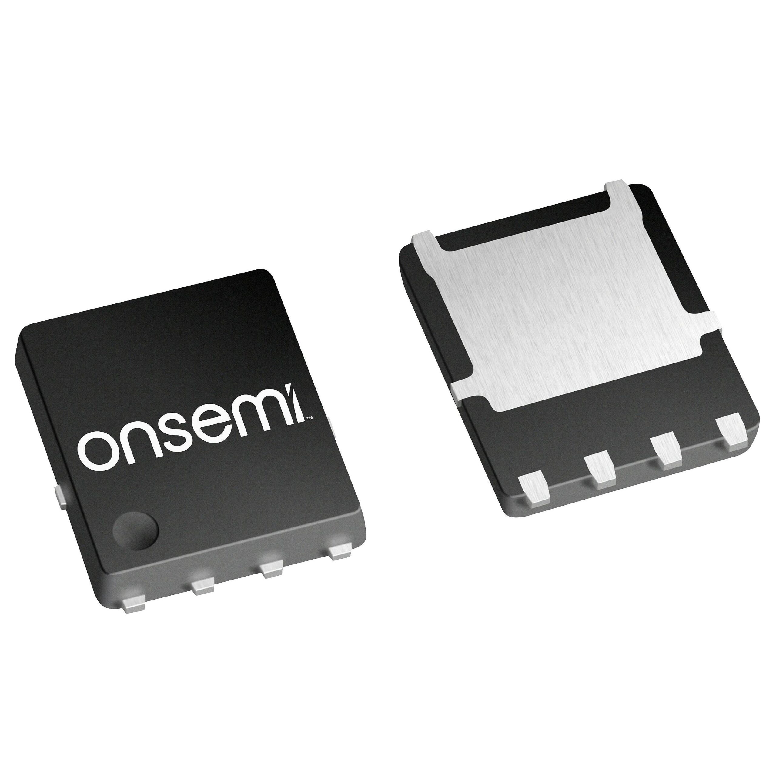
NVMFWS0D63N04XMT1G is listed in the Single FETs, MOSFETs range at ChipApex. The manufacturer field lists onsemi. Its product description is SINGLE N-CHANNEL POWER MOSFET 40. Review the specifications below when checking this part for your BOM.
The onsemi NVMFWS0D63N04XMT1G is a single N-channel power MOSFET in a DFNW5 (SO-8FL) package. It features a drain-to-source voltage of 40 V and a maximum continuous drain current of 384 A at TC = 25 °C. The device has a typical RDS(on) of 0.6 mΩ at VGS = 10 V and ID = 30 A. Total gate charge is typically 92.2 nC. Power dissipation reaches 157 W at TC = 25 °C, with a junction-to-case thermal resistance of 0.95 °C/W. Operating temperature ranges from −55 °C to 175 °C.
Verify the specific ordering suffix against official documentation. The T1G suffix indicates standard tape and reel packaging. Confirm RoHS compliance and Pb-Free status requirements match project specifications. Ensure the DFNW5 package dimensions align with PCB layout constraints before finalizing procurement orders.
Select this component when low conduction loss and high current handling are critical. The 40 V rating suits low-voltage applications. Verify that the gate threshold voltage and total gate charge meet the driving circuit capabilities. Consider the thermal resistance values for adequate heat sinking or copper pad design to maintain safe operating temperatures under load.
This part belongs to the NVMFWS series of single N-channel MOSFETs from onsemi. It utilizes advanced silicon technology to achieve high current density in a small surface-mount package. The SO-8FL form factor provides improved thermal performance compared to traditional packages while maintaining a compact physical profile suitable for modern electronics.
Check datasheets for alternative parts offering similar 40 V ratings and comparable RDS(on) values. Ensure pinout compatibility with the DFNW5 package if direct replacement is required. Verify that thermal characteristics and maximum current ratings meet or exceed the original design requirements.
The maximum pulsed drain current is 900 A for a pulse duration of 10 µs at a case temperature of 25 °C.
Yes, the device is AEC-Q101 qualified and PPAP capable, making it suitable for automotive electronic systems.
The source-to-drain diode forward voltage is typically 0.63 V when the source current is 30 A and the junction temperature is 125 °C.
Explore related parts through FETs, MOSFETs, Transistors, Discrete Semiconductor Products, all product categories.
 NVMFWS0D63N04XMT1G

NVMFWS0D63N04XMT1G is listed in the Single FETs, MOSFETs range at ChipApex. The manufacturer field lists onsemi. Its product description is SINGLE N-CHANNEL POWER MOSFET…
Read More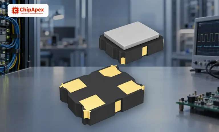
Understand how oscillators generate timing signals, how they differ from crystals, and which frequency, output and stability specs matter when choosing one.
Read More
NVMFWS0D63N04XMT1G is listed in the Single FETs, MOSFETs range at ChipApex. The manufacturer field lists onsemi. Its product description is SINGLE N-CHANNEL POWER MOSFET…
Read More
NVMFWS0D63N04XMT1G is listed in the Single FETs, MOSFETs range at ChipApex. The manufacturer field lists onsemi. Its product description is SINGLE N-CHANNEL POWER MOSFET…
Read More
NVMFWS0D63N04XMT1G is listed in the Single FETs, MOSFETs range at ChipApex. The manufacturer field lists onsemi. Its product description is SINGLE N-CHANNEL POWER MOSFET…
Read More
NVMFWS0D63N04XMT1G is listed in the Single FETs, MOSFETs range at ChipApex. The manufacturer field lists onsemi. Its product description is SINGLE N-CHANNEL POWER MOSFET…
Read More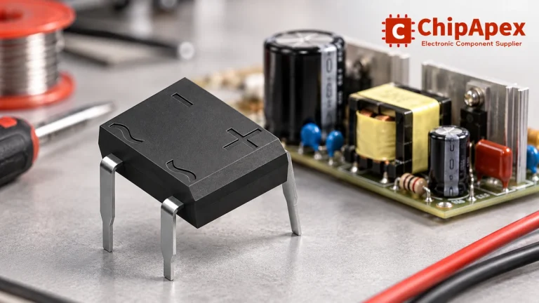
Select a bridge rectifier by reverse voltage, capacitor charging current, startup surge and cooling. Work through a stated DC voltage and ripple example.
Read More
NVMFWS0D63N04XMT1G is listed in the Single FETs, MOSFETs range at ChipApex. The manufacturer field lists onsemi. Its product description is SINGLE N-CHANNEL POWER MOSFET…
Read More
NVMFWS0D63N04XMT1G is listed in the Single FETs, MOSFETs range at ChipApex. The manufacturer field lists onsemi. Its product description is SINGLE N-CHANNEL POWER MOSFET…
Read More
NVMFWS0D63N04XMT1G is listed in the Single FETs, MOSFETs range at ChipApex. The manufacturer field lists onsemi. Its product description is SINGLE N-CHANNEL POWER MOSFET…
Read More
NVMFWS0D63N04XMT1G is listed in the Single FETs, MOSFETs range at ChipApex. The manufacturer field lists onsemi. Its product description is SINGLE N-CHANNEL POWER MOSFET…
Read More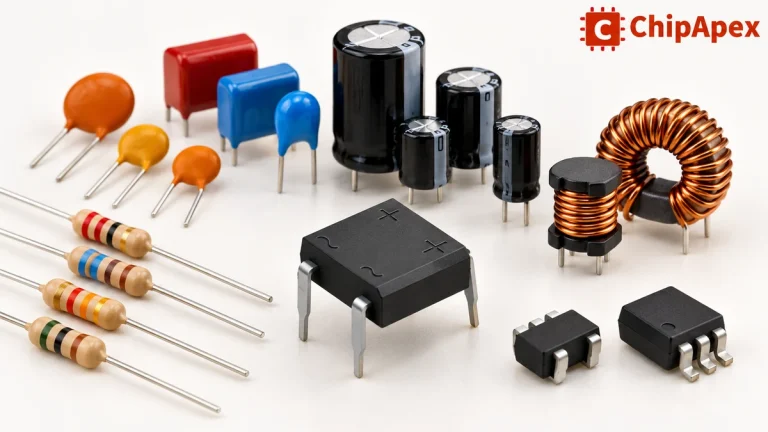
Explore electronic component types, functions, packages and datasheets. Learn selection, replacement and BOM checks before ordering parts for your PCB.
Read More
The activity of extra discounts on wholesale prices is in full swing…
Please fill in your contact information and we will send you the latest wholesale price list.