 ChipApex | Global Electronic Components Supplier

SEARCH
Search Product
Search Post
— IC芯片 | 连接器 | 传感器 | 被动器件 —
Search productSearch post
— IC芯片 | 连接器 | 传感器 | 被动器件 —
Consult the customer manager about the wholesale price.
consultation hotline:86-132-6715-2157
email:[email protected]
Contact the product manager for consultation. One-stop consultation is available.
Do you want a lower wholesale price? Please send us your inquiry and we will reply immediately.
SN74ALS166DRE4 is listed in the Shift Registers range at ChipApex. The manufacturer field lists Texas Instruments. Its product description is IC SHIFT REG 8BIT PARALL 16-SOIC. Review the specifications below when checking this part for your BOM.
The SN74ALS166DRE4 is a parallel-load 8-bit shift register from the Texas Instruments ALS logic family. It operates within a supply voltage range of 4.5 V to 5.5 V and supports a maximum clock frequency of 45 MHz. The device features asynchronous clear, synchronous parallel loading, and serial shifting capabilities. Propagation delays range from 2 ns to 14 ns depending on the signal path. It is housed in a 16-pin SOIC package and functions reliably across an operating temperature range of 0°C to 70°C.
Verify the specific ordering suffix 'E4' against current manufacturer documentation to confirm material composition and compliance status. Confirm the active production status for this exact part number variant before procurement, as legacy ALS series components may have limited availability or obsolescence risks.
Select this component when designing with standard TTL-compatible logic families requiring high-speed shifting. Ensure the system power supply remains strictly between 4.5 V and 5.5 V. Verify that the required clock frequency does not exceed the 45 MHz limit and that the thermal environment stays within the specified 0°C to 70°C operational range.
This device belongs to the SN74ALS166 family of parallel-load 8-bit shift registers. It is characterized for operation from 0°C to 70°C. The 'D' suffix indicates a plastic small-outline package, while 'RE4' denotes specific packaging and environmental compliance attributes defined by the manufacturer.
Consult official datasheets for direct pin-compatible alternatives such as the SN74ALS166DR or SN74ALS166DBR. Verify functional equivalence regarding propagation delays and electrical characteristics before substitution.
The shift/load (SH/LD) input determines the mode. When high, the device accepts serial data at the SER input. When low, parallel data inputs are enabled for synchronous loading on the next clock pulse.
The CLK INH input acts as a clock inhibit. Holding either the CLK or CLK INH input high inhibits clocking, while holding them low enables the other input, allowing the system clock to be stopped on command.
Explore related parts through Logic, Integrated Circuits (ICs), all product categories, ChipApex homepage.
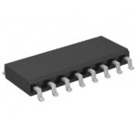 SN74ALS166DRE4
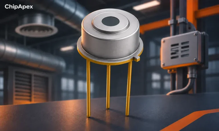
Compare gas sensor technologies, cross-sensitivity and calibration needs. Define the gas, range and environment before choosing a sensing component.
Read More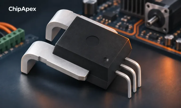
Compare Hall, shunt, current transformer and Rogowski sensing. Check AC/DC capability, accuracy, isolation, heat and response before selecting a sensor.
Read More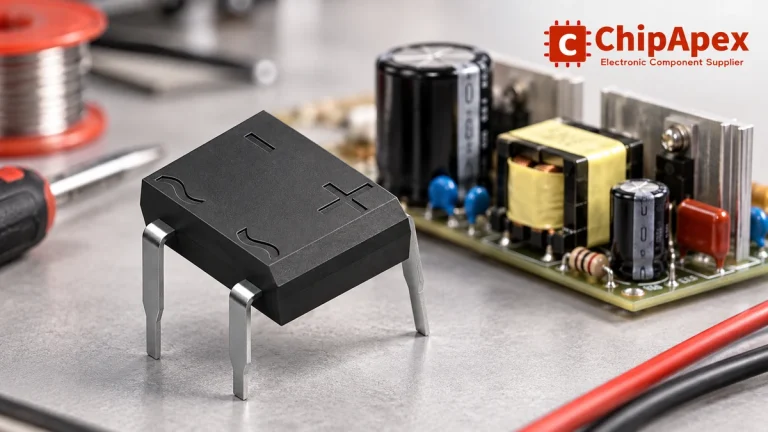
Select a bridge rectifier by reverse voltage, capacitor charging current, startup surge and cooling. Work through a stated DC voltage and ripple example.
Read More
SN74ALS166DRE4 is listed in the Shift Registers range at ChipApex. The manufacturer field lists Texas Instruments. Its product description is IC SHIFT REG 8BIT…
Read More
Compare rheostat and potentiometer wiring and functions. Understand divider loading, wiper current, track power and practical component selection.
Read More
Choose logic inverter ICs by thresholds, supply, output drive and delay. Compare standard and Schmitt-trigger inputs, power sequencing and replacement checks.
Read More
Choose a vibration sensor for machine monitoring. Compare sensing methods, bandwidth, noise and mounting, then define the signal-chain requirements.
Read More
SN74ALS166DRE4 is listed in the Shift Registers range at ChipApex. The manufacturer field lists Texas Instruments. Its product description is IC SHIFT REG 8BIT…
Read More
SN74ALS166DRE4 is listed in the Shift Registers range at ChipApex. The manufacturer field lists Texas Instruments. Its product description is IC SHIFT REG 8BIT…
Read More
Learn how rectifiers convert AC to DC, compare half-wave and bridge circuits, and select voltage, current, recovery and thermal ratings for your design.
Read More
Learn what data acquisition means, from sensors and conditioning to sampling and storage. Review channel timing, wiring, calibration and data quality.
Read More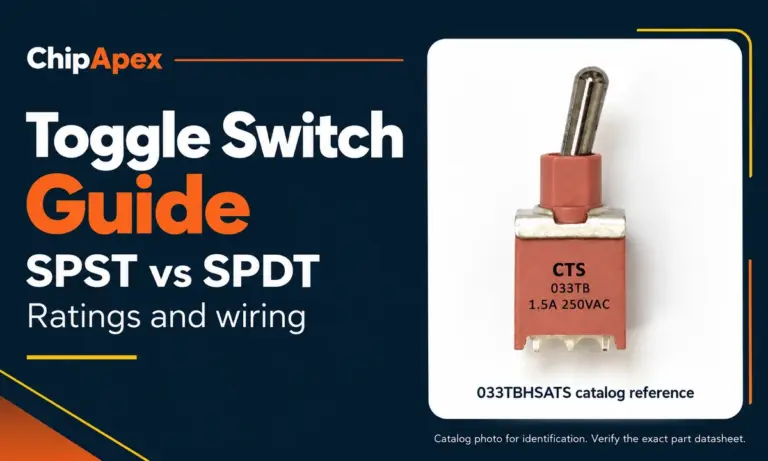
Compare SPST and SPDT toggle switches, understand AC/DC ratings, and follow wiring examples. Check contact action, mounting and parts in the ChipApex catalog.
Read More
The activity of extra discounts on wholesale prices is in full swing…
Please fill in your contact information and we will send you the latest wholesale price list.