 ChipApex | Global Electronic Components Supplier

SEARCH
Search Product
Search Post
— IC芯片 | 连接器 | 传感器 | 被动器件 —
Search productSearch post
— IC芯片 | 连接器 | 传感器 | 被动器件 —
Consult the customer manager about the wholesale price.
consultation hotline:86-132-6715-2157
email:[email protected]
Contact the product manager for consultation. One-stop consultation is available.
Do you want a lower wholesale price? Please send us your inquiry and we will reply immediately.
SN74AUP1G125DSFR is listed in the Buffers, Drivers, Receivers, Transceivers range at ChipApex. The manufacturer field lists Texas Instruments. Its product description is IC BUFFER NON-INVERT 3.6V 6SON. Review the specifications below when checking this part for your BOM.
The SN74AUP1G125DSFR is a low-power single bus buffer gate with 3-state output from the Texas Instruments AUP family. It operates within a supply voltage range of 0.8 V to 3.6 V and supports an operating temperature range of -40°C to +85°C. The device features a maximum propagation delay of 4.6 ns at 3.3 V, low static power consumption (ICC = 0.9 µA maximum), and low dynamic power consumption (Cpd = 4 pF typical). It includes input-disable functionality for floating conditions and Ioff support for partial-power-down mode operation.
Verify the specific package type and tape-and-reel configuration against the manufacturer's current orderable addendum. Confirm that the DSF SON package variant matches the required footprint dimensions and pinout orientation for the target PCB layout. Ensure compliance with RoHS directives and check for any recent manufacturing site changes documented in product change notifications.
Select this component for applications requiring low static and dynamic power consumption across a wide voltage range. It is suitable for mixed-mode signal operations due to its 3.6-V I/O tolerance. Consider the input-disable feature if floating input conditions are possible during system operation. Evaluate thermal performance based on the specific PCB layout and ambient temperature constraints.
This device belongs to the SN74AUP1G series, which represents Texas Instruments' premier solution for low-power needs in battery-powered portable applications. The AUP family is designed to increase battery life while maintaining excellent signal integrity. The SN74AUP1G125 specifically provides a single non-inverting buffer with output enable control.
Direct replacements include other packages of the same logic function such as SN74AUP1G125DBV, SN74AUP1G125DCK, or SN74AUP1G125DRY. Verify pin compatibility and package dimensions before substitution.
The SN74AUP1G125 supports partial-power-down mode through its Ioff circuitry. When the supply voltage drops to 0 V, the inputs and outputs enter a high-impedance state, inhibiting current backflow into the device to prevent damage.
Yes, the device features over-voltage tolerant inputs. Input signals can be driven above the supply voltage, provided they remain below the maximum input voltage value specified in the Absolute Maximum Ratings table.
Explore related parts through Logic, Integrated Circuits (ICs), all product categories, ChipApex homepage.
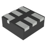 SN74AUP1G125DSFR
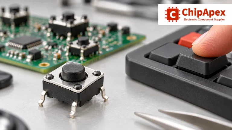
Understand tactile switches, PCB and keyboard differences, four-pin wiring, debounce, force, travel and replacement checks for reliable control inputs.
Read More
SN74AUP1G125DSFR is listed in the Buffers, Drivers, Receivers, Transceivers range at ChipApex. The manufacturer field lists Texas Instruments. Its product description is IC BUFFER…
Read More
SN74AUP1G125DSFR is listed in the Buffers, Drivers, Receivers, Transceivers range at ChipApex. The manufacturer field lists Texas Instruments. Its product description is IC BUFFER…
Read More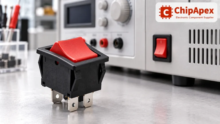
Choose a rocker switch by AC/DC ratings, contact arrangement, illumination, panel fit and sealing. Get practical checks for engineering and component sourcing.
Read More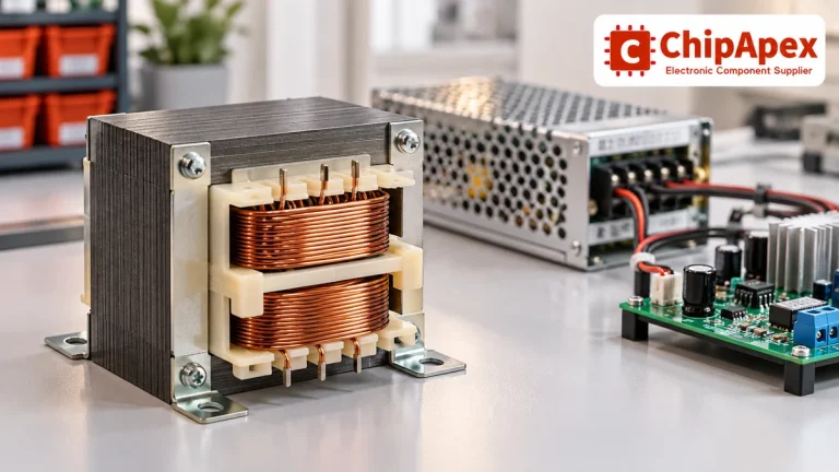
Select power transformers by input frequency, secondary VA, rectifier load, isolation, regulation and inrush. Build a clearer specification for your next RFQ.
Read More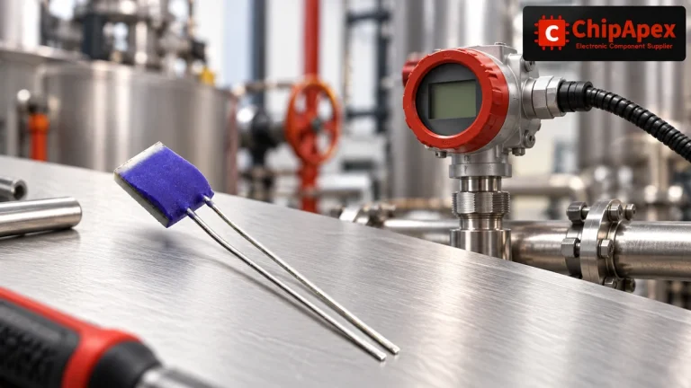
Compare Pt100 and Pt1000 RTDs, two-, three- and four-wire connections, excitation and self-heating. Build an error budget from element to reported temperature.
Read More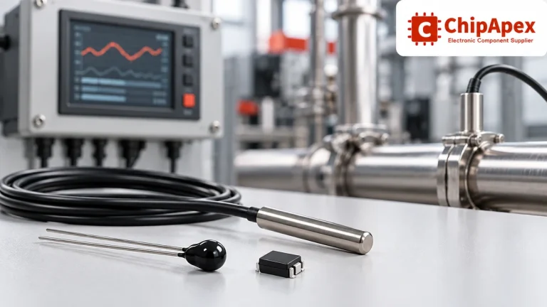
Compare thermistors, RTDs, thermocouples and temperature ICs. Learn how range, accuracy, response, interfaces and mounting affect component selection.
Read More
Understand load cell sensor output, bridge wiring and calibration. Learn how mV/V sensitivity, mechanics and ADC noise affect measurement accuracy.
Read More
SN74AUP1G125DSFR is listed in the Buffers, Drivers, Receivers, Transceivers range at ChipApex. The manufacturer field lists Texas Instruments. Its product description is IC BUFFER…
Read More
Learn how to use ferrite beads for noise filtering. Check impedance, DC bias, placement, resonance and load-step behavior before selecting a part.
Read More
SN74AUP1G125DSFR is listed in the Buffers, Drivers, Receivers, Transceivers range at ChipApex. The manufacturer field lists Texas Instruments. Its product description is IC BUFFER…
Read More
Choose a vibration sensor for machine monitoring. Compare sensing methods, bandwidth, noise and mounting, then define the signal-chain requirements.
Read More
The activity of extra discounts on wholesale prices is in full swing…
Please fill in your contact information and we will send you the latest wholesale price list.





