 ChipApex | Global Electronic Components Supplier

SEARCH
Search Product
Search Post
— IC芯片 | 连接器 | 传感器 | 被动器件 —
Search productSearch post
— IC芯片 | 连接器 | 传感器 | 被动器件 —
Consult the customer manager about the wholesale price.
consultation hotline:86-132-6715-2157
email:[email protected]
Contact the product manager for consultation. One-stop consultation is available.
Do you want a lower wholesale price? Please send us your inquiry and we will reply immediately.
SN74AVC4T245DGVR is listed in the Buffers, Drivers, Receivers, Transceivers range at ChipApex. The manufacturer field lists Texas Instruments. Its product description is IC TRANSLATION TXRX 3.6V 16TVSOP. Review the specifications below when checking this part for your BOM.
The SN74AVC4T245DGVR is a 4-bit dual-supply noninverting bus transceiver with configurable voltage translation and 3-state outputs. It operates within a supply voltage range of 1.2V to 3.6V on both VCCA and VCCB rails. The device supports maximum data rates up to 380Mbps for 1.8V to 3.3V translation. It features I/Os that are 4.6V tolerant and includes Ioff circuitry for partial power-down mode operation. The component utilizes a TVSOP-16 package.
Verify the specific ordering suffix DGVR corresponds to the TVSOP-16 package and tape-and-reel shipping configuration. Confirm RoHS compliance status and SVHC declarations against the latest manufacturer documentation before integration. Ensure input pins are held at valid logic levels to prevent excess current consumption during operation.
Select this component when asynchronous communication between two data buses requires voltage level translation across different supply rails. It is suitable for interfacing devices operating at distinct interface voltages, such as translating between 1.2V, 1.5V, 1.8V, 2.5V, and 3.3V nodes. Ensure the application does not exceed the 4.6V I/O tolerance rating.
This device belongs to the SN74AVC4T245 family of 4-bit dual-supply bus transceivers. The family offers identical electrical functionality across multiple package options, including SOIC, TSSOP, WQFN, UQFN, SOT, and TVSOP configurations. The DGVR suffix specifically identifies the Thin-shrink small-outline package variant designed for surface-mount assembly.
SN74AVC4T245DGV
To place outputs in the high-impedance state during power-up or power-down, the OE input must be tied to VCCA through a pullup resistor. This prevents enabling until VCCA and VCCB are fully ramped and stable.
The Ioff feature supports partial-power-down mode by disabling the I/O output circuits. This prevents damaging current backflow through the device when it is powered down but connected to active systems.
Explore related parts through Logic, Integrated Circuits (ICs), all product categories, ChipApex homepage.
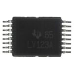 SN74AVC4T245DGVR
Compare RC, crystal and MEMS oscillator circuits. Check ppm, jitter, load capacitance, startup margin and output compatibility before choosing a clock source.
Read More
SN74AVC4T245DGVR is listed in the Buffers, Drivers, Receivers, Transceivers range at ChipApex. The manufacturer field lists Texas Instruments. Its product description is IC TRANSLATION…
Read More
Learn how a JFET works and how to compare bias, leakage, noise and pinout. Review practical selection questions for high-impedance analog circuits.
Read More
SN74AVC4T245DGVR is listed in the Buffers, Drivers, Receivers, Transceivers range at ChipApex. The manufacturer field lists Texas Instruments. Its product description is IC TRANSLATION…
Read More
Choose logic inverter ICs by thresholds, supply, output drive and delay. Compare standard and Schmitt-trigger inputs, power sequencing and replacement checks.
Read More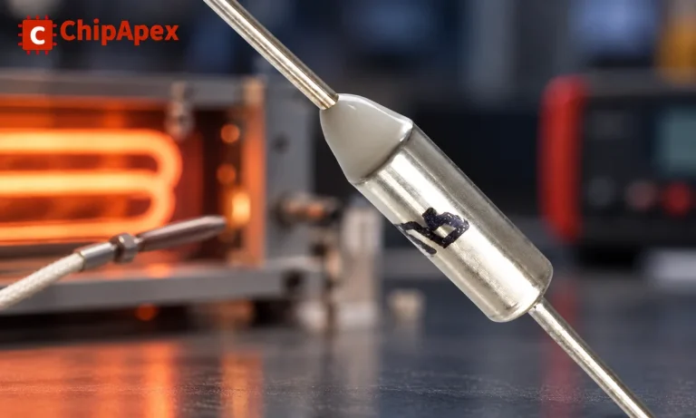
Understand thermal fuse operation, Tf, Th and Tm, electrical ratings and mounting. Check temperature limits and replacement requirements for your design.
Read More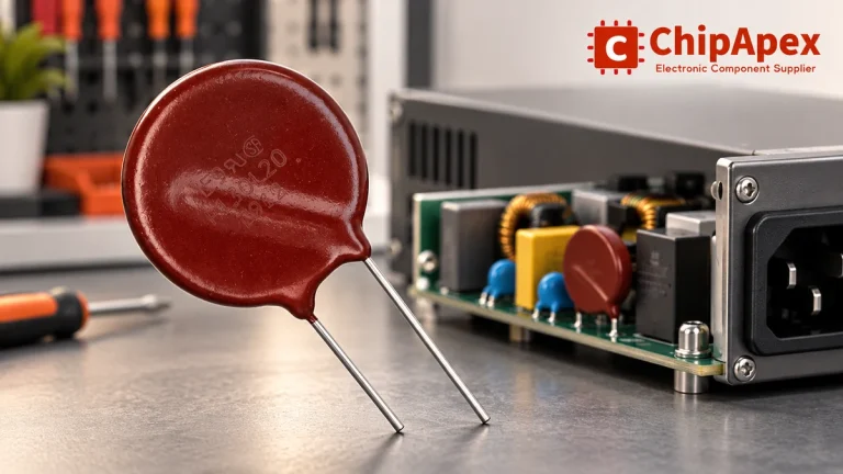
Select MOV varistors by continuous voltage, clamping behavior, surge waveform and repetition. Check thermal disconnection, fuse coordination and replacements.
Read More
SN74AVC4T245DGVR is listed in the Buffers, Drivers, Receivers, Transceivers range at ChipApex. The manufacturer field lists Texas Instruments. Its product description is IC TRANSLATION…
Read More
SN74AVC4T245DGVR is listed in the Buffers, Drivers, Receivers, Transceivers range at ChipApex. The manufacturer field lists Texas Instruments. Its product description is IC TRANSLATION…
Read More
SN74AVC4T245DGVR is listed in the Buffers, Drivers, Receivers, Transceivers range at ChipApex. The manufacturer field lists Texas Instruments. Its product description is IC TRANSLATION…
Read More
SN74AVC4T245DGVR is listed in the Buffers, Drivers, Receivers, Transceivers range at ChipApex. The manufacturer field lists Texas Instruments. Its product description is IC TRANSLATION…
Read More
SN74AVC4T245DGVR is listed in the Buffers, Drivers, Receivers, Transceivers range at ChipApex. The manufacturer field lists Texas Instruments. Its product description is IC TRANSLATION…
Read More
The activity of extra discounts on wholesale prices is in full swing…
Please fill in your contact information and we will send you the latest wholesale price list.





