 ChipApex | Global Electronic Components Supplier

SEARCH
Search Product
Search Post
— IC芯片 | 连接器 | 传感器 | 被动器件 —
Search productSearch post
— IC芯片 | 连接器 | 传感器 | 被动器件 —
Consult the customer manager about the wholesale price.
consultation hotline:86-132-6715-2157
email:[email protected]
Contact the product manager for consultation. One-stop consultation is available.
Do you want a lower wholesale price? Please send us your inquiry and we will reply immediately.
SN74HC126PWR is listed in the Buffers, Drivers, Receivers, Transceivers range at ChipApex. The manufacturer field lists Texas Instruments. Its product description is IC BUFFER NON-INVERT 6V 14TSSOP. Review the specifications below when checking this part for your BOM.
The SN74HC126PWR is a quadruple buffer with 3-state outputs manufactured by Texas Instruments. It operates within a supply voltage range of 2 V to 6 V and supports an operating temperature range of -40°C to +85°C. The device features buffered inputs, balanced CMOS outputs capable of sinking and sourcing similar currents, and standard high-impedance CMOS inputs. It provides fanout support for up to 10 LSTTL loads while offering significant power reduction compared to LSTTL logic ICs.
Verify the specific package type matches the design requirements, as the SN74HC126 family includes SOIC, SSOP, PDIP, SO, TSSOP, CDIP, and LCCC options. Confirm that the ordering suffix corresponds to the desired packaging format, such as tape and reel or tube, as these do not alter the internal function but affect handling and assembly processes.
Select this component when a non-inverting buffer with controllable output states is required. Ensure the application voltage falls between 2 V and 6 V. Consider the thermal resistance metrics provided in the datasheet if high current loads are anticipated. Unused inputs must be terminated to VCC or ground to prevent undefined operational states.
This part belongs to the SNx4HC126 series of quadruple bus buffer gates. It is designed for general-purpose digital logic applications requiring signal buffering and bus control. The device is compatible with standard CMOS logic families and offers improved performance over older LSTTL technologies regarding power consumption.
SN74HC126D
Unused inputs must be terminated to either VCC or ground. They can be directly terminated if completely unused or connected with a pull-up/pull-down resistor if used intermittently.
When disabled, the output enters a high-impedance state where it neither sources nor sinks current. The output voltage is then determined by the external circuit connected to the pin.
Explore related parts through Logic, Integrated Circuits (ICs), all product categories, ChipApex homepage.
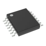 SN74HC126PWR

SN74HC126PWR is listed in the Buffers, Drivers, Receivers, Transceivers range at ChipApex. The manufacturer field lists Texas Instruments. Its product description is IC BUFFER…
Read More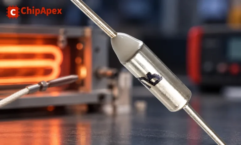
Understand thermal fuse operation, Tf, Th and Tm, electrical ratings and mounting. Check temperature limits and replacement requirements for your design.
Read More
SN74HC126PWR is listed in the Buffers, Drivers, Receivers, Transceivers range at ChipApex. The manufacturer field lists Texas Instruments. Its product description is IC BUFFER…
Read More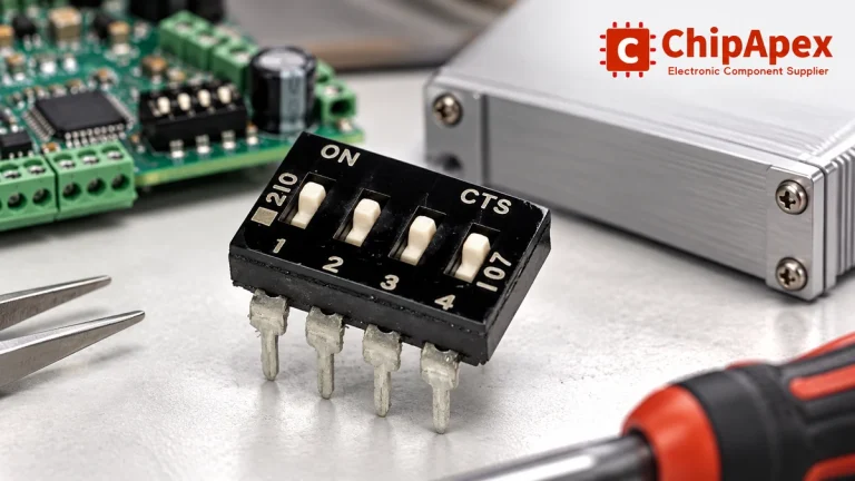
Choose a DIP switch by contact type, coded positions, footprint and signal ratings. Check logic polarity, assembly conditions and PCB configuration behavior.
Read More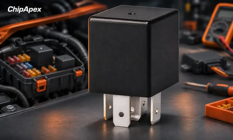
Understand automotive relay terminals, coil suppression and load ratings. Check inrush, socket compatibility and temperature before selecting a replacement.
Read More
SN74HC126PWR is listed in the Buffers, Drivers, Receivers, Transceivers range at ChipApex. The manufacturer field lists Texas Instruments. Its product description is IC BUFFER…
Read More
SN74HC126PWR is listed in the Buffers, Drivers, Receivers, Transceivers range at ChipApex. The manufacturer field lists Texas Instruments. Its product description is IC BUFFER…
Read More
SN74HC126PWR is listed in the Buffers, Drivers, Receivers, Transceivers range at ChipApex. The manufacturer field lists Texas Instruments. Its product description is IC BUFFER…
Read More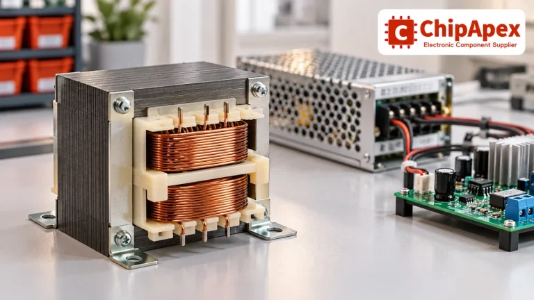
Select power transformers by input frequency, secondary VA, rectifier load, isolation, regulation and inrush. Build a clearer specification for your next RFQ.
Read More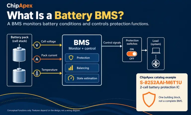
Learn what a battery BMS does, how protection differs from charging, and which pack specifications to check when sourcing BMS components through ChipApex.
Read More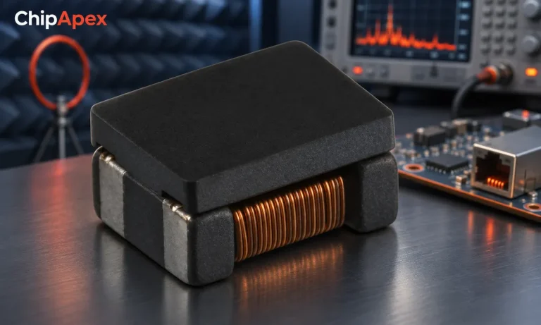
Select a common mode choke using noise frequency, current, insulation and signal integrity. Understand impedance curves, layout and filter limitations.
Read More
SN74HC126PWR is listed in the Buffers, Drivers, Receivers, Transceivers range at ChipApex. The manufacturer field lists Texas Instruments. Its product description is IC BUFFER…
Read More
The activity of extra discounts on wholesale prices is in full swing…
Please fill in your contact information and we will send you the latest wholesale price list.





