 ChipApex | Global Electronic Components Supplier

SEARCH
Search Product
Search Post
— IC芯片 | 连接器 | 传感器 | 被动器件 —
Search productSearch post
— IC芯片 | 连接器 | 传感器 | 被动器件 —
Consult the customer manager about the wholesale price.
consultation hotline:86-132-6715-2157
email:[email protected]
Contact the product manager for consultation. One-stop consultation is available.
Do you want a lower wholesale price? Please send us your inquiry and we will reply immediately.
SN74HC365PWR is listed in the Buffers, Drivers, Receivers, Transceivers range at ChipApex. The manufacturer field lists Texas Instruments. Its product description is IC BUFFER NON-INVERT 6V 16TSSOP. Review the specifications below when checking this part for your BOM.
The SN74HC365PWR is a hex buffer and line driver with 3-state outputs manufactured by Texas Instruments. It operates within a supply voltage range of 2 V to 6 V and supports an operating temperature range from -40°C to +85°C. The device features six independent non-inverting buffers, each capable of driving bus lines or up to 15 LSTTL loads. Key electrical characteristics include a maximum propagation delay of 20 ns at 6 V, typical output drive currents of ±6 mA at 5 V, and a maximum quiescent current of 80 µA.
Verify the specific package type TSSOP-16 and ensure compatibility with the recommended operating conditions including the 2 V to 6 V supply voltage range. Confirm that the moisture sensitivity level and reflow temperature profiles align with your assembly process requirements before finalizing procurement.
Select this component when designing systems requiring multiple buffered outputs with tri-state capability for bus sharing. Ensure the application logic correctly manages the OE1 and OE2 pins to prevent contention on shared buses. Verify that the load capacitance does not exceed specifications to maintain signal integrity.
This part belongs to the SNx4HC365 family of hex buffers and line drivers. It is distinct from other variants like the SN74HCS365 which offers different power and speed characteristics. The 'PWR' suffix specifically denotes the TSSOP surface-mount package with tape and reel shipping configuration.
SN74HC365DR
Outputs enter a high-impedance state if either OE1 or OE2 is set to a high state. Data passes from inputs to outputs only when both enable pins are low.
All unused inputs must be connected to either VCC or GND to prevent undefined operational states caused by floating voltages.
Explore related parts through Logic, Integrated Circuits (ICs), all product categories, ChipApex homepage.
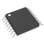 SN74HC365PWR
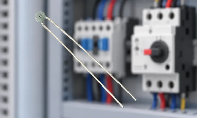
Learn why PTC resistance rises with temperature, how it differs from NTC, and which ratings matter for sensing and protection.
Read More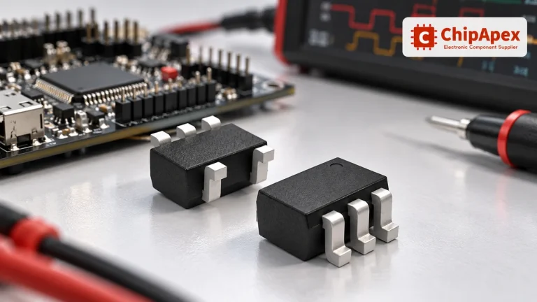
Choose logic inverter ICs by thresholds, supply, output drive and delay. Compare standard and Schmitt-trigger inputs, power sequencing and replacement checks.
Read More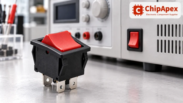
Choose a rocker switch by AC/DC ratings, contact arrangement, illumination, panel fit and sealing. Get practical checks for engineering and component sourcing.
Read More
SN74HC365PWR is listed in the Buffers, Drivers, Receivers, Transceivers range at ChipApex. The manufacturer field lists Texas Instruments. Its product description is IC BUFFER…
Read More
Learn how a TRIAC switches AC loads. Understand triggering, latching, holding current, phase control and thermal limits before choosing a component.
Read More
SN74HC365PWR is listed in the Buffers, Drivers, Receivers, Transceivers range at ChipApex. The manufacturer field lists Texas Instruments. Its product description is IC BUFFER…
Read More
SN74HC365PWR is listed in the Buffers, Drivers, Receivers, Transceivers range at ChipApex. The manufacturer field lists Texas Instruments. Its product description is IC BUFFER…
Read More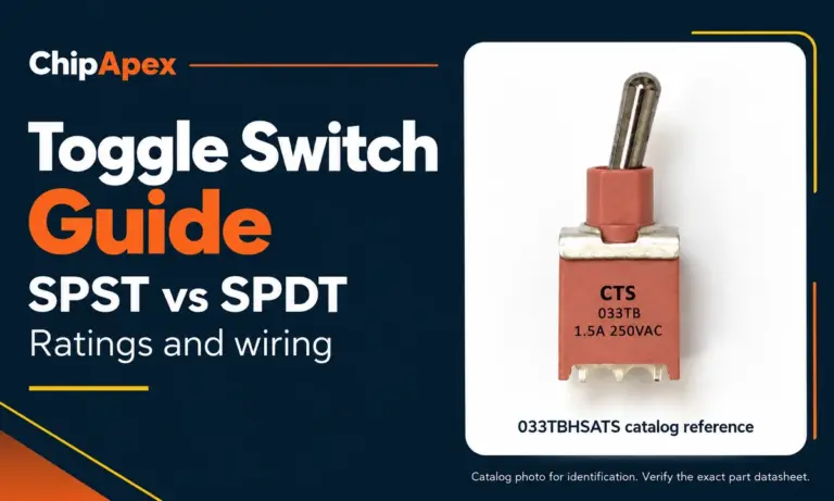
Compare SPST and SPDT toggle switches, understand AC/DC ratings, and follow wiring examples. Check contact action, mounting and parts in the ChipApex catalog.
Read More
Learn how an analog front end conditions sensor signals. Compare gain, noise, filtering, ADC settling and integration options before selecting components.
Read More
Compare Pt100 and Pt1000 RTDs, two-, three- and four-wire connections, excitation and self-heating. Build an error budget from element to reported temperature.
Read More
See how a MEMS gyroscope measures angular rate, why its angle estimate drifts, and which range, noise, interface and temperature specs to compare.
Read More
SN74HC365PWR is listed in the Buffers, Drivers, Receivers, Transceivers range at ChipApex. The manufacturer field lists Texas Instruments. Its product description is IC BUFFER…
Read More
The activity of extra discounts on wholesale prices is in full swing…
Please fill in your contact information and we will send you the latest wholesale price list.





