 ChipApex | Global Electronic Components Supplier

SEARCH
Search Product
Search Post
— IC芯片 | 连接器 | 传感器 | 被动器件 —
Search productSearch post
— IC芯片 | 连接器 | 传感器 | 被动器件 —
Consult the customer manager about the wholesale price.
consultation hotline:86-132-6715-2157
email:[email protected]
Contact the product manager for consultation. One-stop consultation is available.
Do you want a lower wholesale price? Please send us your inquiry and we will reply immediately.
SN74LV125APWRG4 is listed in the Buffers, Drivers, Receivers, Transceivers range at ChipApex. The manufacturer field lists Texas Instruments. Its product description is IC BUF NON-INVERT 5.5V 14TSSOP. Review the specifications below when checking this part for your BOM.
The SN74LV125APWRG4 is a quad bus buffer gate manufactured by Texas Instruments. It operates within a supply voltage range of 2.0 V to 5.5 V and features four non-inverting inputs with three-state outputs. The device utilizes LV logic technology and is housed in a TSSOP-14 surface-mount package. It supports single-ended input types and provides high-level output current up to -16 mA and low-level output current up to 16 mA. Propagation delay is specified at 16.5 ns under 2.5 V conditions with a 50 pF load. The component functions reliably across an operating temperature range from -40°C to +85°C.
Verify the specific suffix 'A' against official datasheets, as it may indicate automotive qualification or specific manufacturing lot variations distinct from standard commercial grades. Confirm RoHS compliance status directly with the manufacturer documentation. Ensure the TSSOP-14 package dimensions match your PCB footprint requirements precisely before finalizing procurement decisions.
Select this component when designing systems requiring robust signal buffering with controlled propagation delays. The wide voltage tolerance allows compatibility with various power rails. Consider the thermal performance and pinout configuration relative to alternative packages like SOIC or VQFN if space constraints exist. Evaluate the drive strength requirements against the specified 16 mA output capability.
This part belongs to the SN74LV125 family of quad bus buffers. It shares functional similarities with other members like the SN74LV125ATRGYRG4 but differs in packaging and potentially qualification standards. The LV series offers improved switching speeds compared to older HC families while maintaining CMOS compatibility. It serves as a critical interface component in digital logic circuits requiring signal isolation or level shifting.
The maximum operating supply voltage is 5.5 V.
Yes, the wide supply voltage range allows it to function in systems requiring voltage translation between different logic levels.
Explore related parts through Logic, Integrated Circuits (ICs), all product categories, ChipApex homepage.
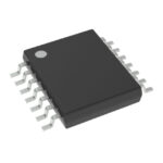 SN74LV125APWRG4
Select a DC-DC converter by input range, topology, isolation and temperature. Compare ripple, efficiency and load limits before choosing a component.
Read More
Understand load cell sensor output, bridge wiring and calibration. Learn how mV/V sensitivity, mechanics and ADC noise affect measurement accuracy.
Read More
See how a MEMS gyroscope measures angular rate, why its angle estimate drifts, and which range, noise, interface and temperature specs to compare.
Read More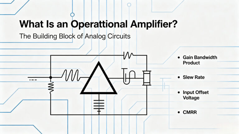
SN74LV125APWRG4 is listed in the Buffers, Drivers, Receivers, Transceivers range at ChipApex. The manufacturer field lists Texas Instruments. Its product description is IC BUF…
Read More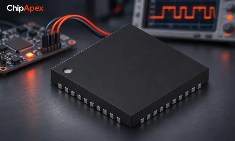
Understand UART protocol framing, baud rate and electrical interfaces. Learn 8N1 timing, TX/RX wiring, buffering and practical troubleshooting steps.
Read More
SN74LV125APWRG4 is listed in the Buffers, Drivers, Receivers, Transceivers range at ChipApex. The manufacturer field lists Texas Instruments. Its product description is IC BUF…
Read More
SN74LV125APWRG4 is listed in the Buffers, Drivers, Receivers, Transceivers range at ChipApex. The manufacturer field lists Texas Instruments. Its product description is IC BUF…
Read More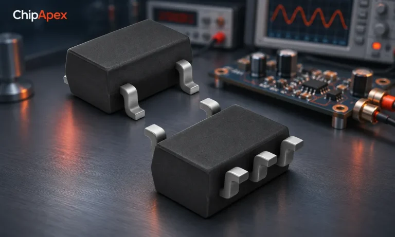
Learn how a JFET works and how to compare bias, leakage, noise and pinout. Review practical selection questions for high-impedance analog circuits.
Read More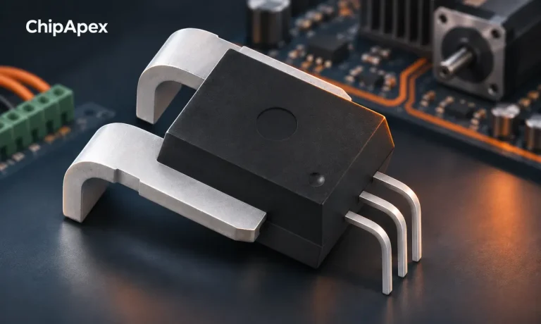
Compare Hall, shunt, current transformer and Rogowski sensing. Check AC/DC capability, accuracy, isolation, heat and response before selecting a sensor.
Read More
SN74LV125APWRG4 is listed in the Buffers, Drivers, Receivers, Transceivers range at ChipApex. The manufacturer field lists Texas Instruments. Its product description is IC BUF…
Read More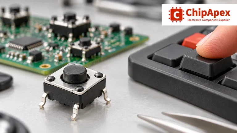
Understand tactile switches, PCB and keyboard differences, four-pin wiring, debounce, force, travel and replacement checks for reliable control inputs.
Read More
SN74LV125APWRG4 is listed in the Buffers, Drivers, Receivers, Transceivers range at ChipApex. The manufacturer field lists Texas Instruments. Its product description is IC BUF…
Read More
The activity of extra discounts on wholesale prices is in full swing…
Please fill in your contact information and we will send you the latest wholesale price list.





