 ChipApex | Global Electronic Components Supplier

SEARCH
Search Product
Search Post
— IC芯片 | 连接器 | 传感器 | 被动器件 —
Search productSearch post
— IC芯片 | 连接器 | 传感器 | 被动器件 —
Consult the customer manager about the wholesale price.
consultation hotline:86-132-6715-2157
email:[email protected]
Contact the product manager for consultation. One-stop consultation is available.
Do you want a lower wholesale price? Please send us your inquiry and we will reply immediately.
SN74LV126ADR is listed in the Buffers, Drivers, Receivers, Transceivers range at ChipApex. The manufacturer field lists Texas Instruments. Its product description is IC BUF NON-INVERT 5.5V 14SOIC. Review the specifications below when checking this part for your BOM.
The SN74LV126ADR is a quadruple bus buffer gate with 3-state outputs manufactured by Texas Instruments. It operates within a supply voltage range of 2V to 5.5V and supports mixed-mode voltage operation on all ports. The device features independent line drivers where each output is disabled when the associated output-enable (OE) input is low. It provides a maximum propagation delay of 6.5ns at 5V and includes Ioff support for live insertion, partial power down mode, and back drive protection.
Verify that the component matches the SN74LV126A family specifications before integration. Confirm the package type corresponds to the SOIC-14 designation indicated by the 'D' suffix in the part number. Ensure compatibility with the required operating temperature range of -40°C to 125°C. Check for RoHS compliance status if environmental regulations apply to the specific manufacturing batch.
Select this component for applications requiring bus buffering with 3-state control and mixed-voltage interface capabilities. It is suitable for designs needing live insertion support and protection against back driving. Consider the wide operating voltage range from 2V to 5.5V when interfacing with various logic families. Evaluate the propagation delay characteristics relative to system timing requirements.
This device belongs to the SN74LV126A series of quadruple bus buffer gates. It is designed for low-drive CMOS applications where output ringing is a concern due to its slow edge rates. The inputs are 5.5V tolerant at any valid VCC, making it effective for translating signals down to lower voltage domains. It utilizes standard digital logic interfaces with active-high enable controls.
SN74LV126ADBR
The device supports partial power down modes through its Ioff feature, which prevents current flow from the outputs when the device is powered down.
The Output Enable (OE) input controls the state of the buffers. When OE is low, the respective output is disabled and enters a high-impedance state. When OE is high, the gate passes data from the A input to the Y output.
Explore related parts through Logic, Integrated Circuits (ICs), all product categories, ChipApex homepage.
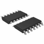 SN74LV126ADR

SN74LV126ADR is listed in the Buffers, Drivers, Receivers, Transceivers range at ChipApex. The manufacturer field lists Texas Instruments. Its product description is IC BUF…
Read More
SN74LV126ADR is listed in the Buffers, Drivers, Receivers, Transceivers range at ChipApex. The manufacturer field lists Texas Instruments. Its product description is IC BUF…
Read More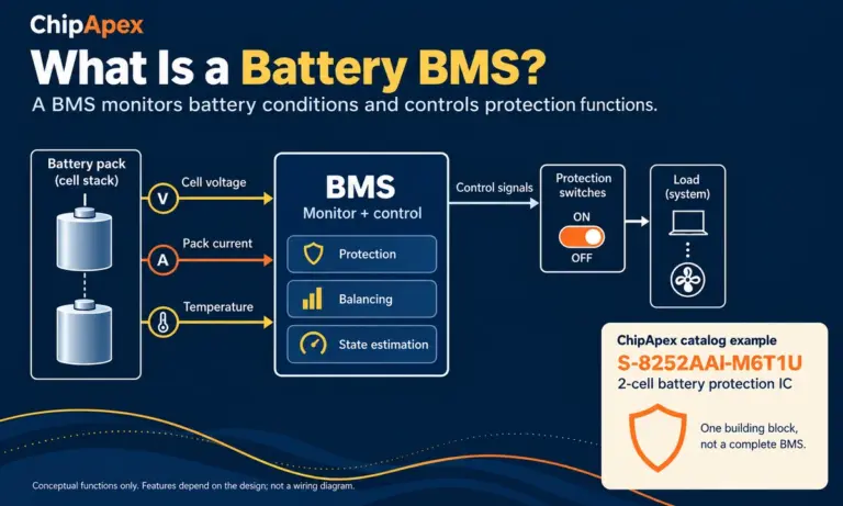
Learn what a battery BMS does, how protection differs from charging, and which pack specifications to check when sourcing BMS components through ChipApex.
Read More
Learn how a diode conducts, how to identify anode and cathode, and when to choose rectifier, TVS, Zener or photodiode types for a circuit.
Read More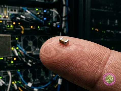
SN74LV126ADR is listed in the Buffers, Drivers, Receivers, Transceivers range at ChipApex. The manufacturer field lists Texas Instruments. Its product description is IC BUF…
Read More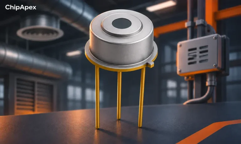
Compare gas sensor technologies, cross-sensitivity and calibration needs. Define the gas, range and environment before choosing a sensing component.
Read More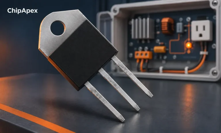
Learn how a TRIAC switches AC loads. Understand triggering, latching, holding current, phase control and thermal limits before choosing a component.
Read More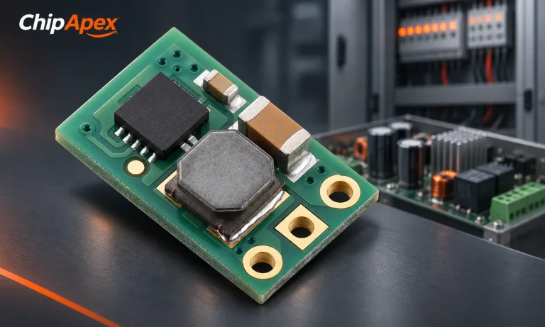
Select a DC-DC converter by input range, topology, isolation and temperature. Compare ripple, efficiency and load limits before choosing a component.
Read More
SN74LV126ADR is listed in the Buffers, Drivers, Receivers, Transceivers range at ChipApex. The manufacturer field lists Texas Instruments. Its product description is IC BUF…
Read More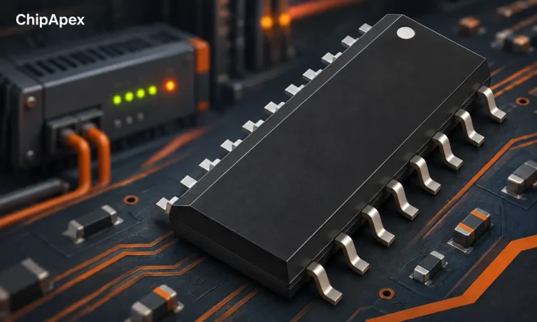
Learn what a shift register does, how bits move and when to use SIPO or PISO devices. Review latch timing, logic levels, output drive…
Read More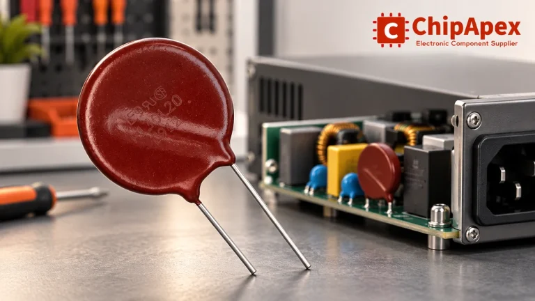
Select MOV varistors by continuous voltage, clamping behavior, surge waveform and repetition. Check thermal disconnection, fuse coordination and replacements.
Read More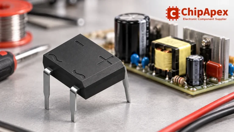
Select a bridge rectifier by reverse voltage, capacitor charging current, startup surge and cooling. Work through a stated DC voltage and ripple example.
Read More
The activity of extra discounts on wholesale prices is in full swing…
Please fill in your contact information and we will send you the latest wholesale price list.





