 ChipApex | Global Electronic Components Supplier

SEARCH
Search Product
Search Post
— IC芯片 | 连接器 | 传感器 | 被动器件 —
Search productSearch post
— IC芯片 | 连接器 | 传感器 | 被动器件 —
Consult the customer manager about the wholesale price.
consultation hotline:86-132-6715-2157
email:[email protected]
Contact the product manager for consultation. One-stop consultation is available.
Do you want a lower wholesale price? Please send us your inquiry and we will reply immediately.
SN74LV165ADBR is listed in the Shift Registers range at ChipApex. The manufacturer field lists Texas Instruments. Its product description is IC REGISTR PAR-LOAD 8BIT 16SSOP. Review the specifications below when checking this part for your BOM.
The SN74LV165ADBR is a parallel-load, 8-bit shift register from the Texas Instruments SN74LV series. It operates within a supply voltage range of 2 V to 5.5 V and supports mixed-mode voltage operation on all ports. The device features balanced CMOS push-pull outputs and includes clock-inhibit functionality alongside a complemented serial output (QH). Designed for surface-mount applications, it utilizes a 16-SSOP package. The component incorporates Ioff circuitry to support partial-power-down modes by disabling outputs to prevent damaging current backflow when powered down.
Verify that the specific ordering suffix 'DBR' corresponds to the SSOP package and tape-and-reel packaging format as documented in the manufacturer's orderable addendum. Confirm that the component meets RoHS3 compliance standards and matches the exact SN74LV165A functional specification before integration into production designs.
Select this component when an 8-bit parallel-to-serial conversion capability is required within a 2 V to 5.5 V operating environment. Ensure the design accommodates the 16-SSOP footprint dimensions. Consider the mixed-mode voltage support if interfacing with logic families operating at different voltage levels than the primary supply.
This part belongs to the SN74LV family of low-voltage CMOS logic devices manufactured by Texas Instruments. The SN74LV165A variant specifically provides parallel-load shift register functionality. The 'DBR' suffix indicates the physical package configuration and reel packaging method, distinguishing it from other variants such as SOIC or TSSOP packages within the same logical family.
SN74LV165ADBRG4
Holding the SH/LD input at a low level enables parallel access to the eight individual direct data inputs, allowing immediate loading of data into the internal registers.
The CLK INH pin serves as a clock-inhibit function. Clocking occurs via a low-to-high transition of the CLK input while CLK INH is held low, or vice versa, allowing interchangeable use of these control signals.
Explore related parts through Logic, Integrated Circuits (ICs), all product categories, ChipApex homepage.
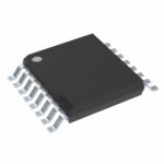 SN74LV165ADBR
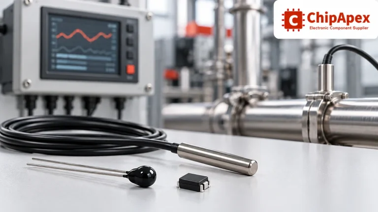
Compare thermistors, RTDs, thermocouples and temperature ICs. Learn how range, accuracy, response, interfaces and mounting affect component selection.
Read More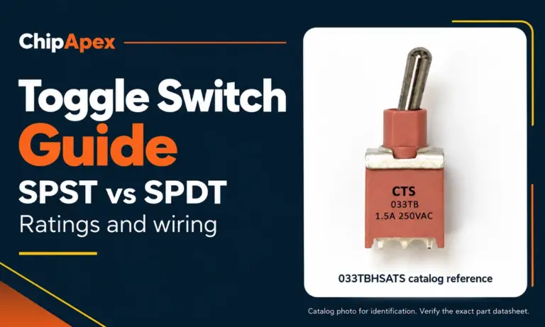
Compare SPST and SPDT toggle switches, understand AC/DC ratings, and follow wiring examples. Check contact action, mounting and parts in the ChipApex catalog.
Read More
Find out when a bare shock switch needs a pull resistor, when an MCU internal pull-up is enough, and why sensor modules and piezo…
Read More
SN74LV165ADBR is listed in the Shift Registers range at ChipApex. The manufacturer field lists Texas Instruments. Its product description is IC REGISTR PAR-LOAD 8BIT…
Read More
SN74LV165ADBR is listed in the Shift Registers range at ChipApex. The manufacturer field lists Texas Instruments. Its product description is IC REGISTR PAR-LOAD 8BIT…
Read More
Understand RF attenuator dB values, fixed and programmable types, impedance, power limits and noise tradeoffs before choosing parts for an RF signal path.
Read More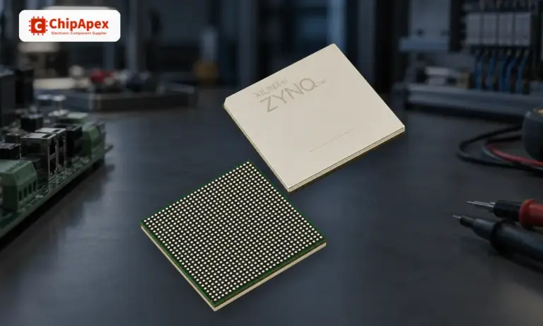
Learn what an integrated circuit is, how ICs work, the main types and the specs to check before choosing a part for your design…
Read More
SN74LV165ADBR is listed in the Shift Registers range at ChipApex. The manufacturer field lists Texas Instruments. Its product description is IC REGISTR PAR-LOAD 8BIT…
Read More
SN74LV165ADBR is listed in the Shift Registers range at ChipApex. The manufacturer field lists Texas Instruments. Its product description is IC REGISTR PAR-LOAD 8BIT…
Read More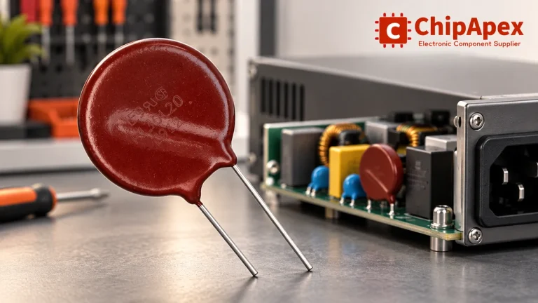
Select MOV varistors by continuous voltage, clamping behavior, surge waveform and repetition. Check thermal disconnection, fuse coordination and replacements.
Read More
Understand how a comparator switches at a voltage threshold, why hysteresis prevents chatter, and which output and input specs matter.
Read More
SN74LV165ADBR is listed in the Shift Registers range at ChipApex. The manufacturer field lists Texas Instruments. Its product description is IC REGISTR PAR-LOAD 8BIT…
Read More
The activity of extra discounts on wholesale prices is in full swing…
Please fill in your contact information and we will send you the latest wholesale price list.






