 ChipApex | Global Electronic Components Supplier

SEARCH
Search Product
Search Post
— IC芯片 | 连接器 | 传感器 | 被动器件 —
Search productSearch post
— IC芯片 | 连接器 | 传感器 | 被动器件 —
Consult the customer manager about the wholesale price.
consultation hotline:86-132-6715-2157
email:[email protected]
Contact the product manager for consultation. One-stop consultation is available.
Do you want a lower wholesale price? Please send us your inquiry and we will reply immediately.
SN74LVC7001APWRQ1 is listed in the Inverter Gates range at ChipApex. The manufacturer field lists Texas Instruments. Its product description is AUTOMOTIVE QUADRUPLE TWO-INPUT 1. Review the specifications below when checking this part for your BOM.
The SN74LVC7001A-Q1 is an automotive-grade quad two-input AND gate featuring Schmitt-trigger inputs. It operates within a supply voltage range of 1.1V to 3.6V and supports 5.5V tolerant input pins. The device provides balanced CMOS push-pull outputs capable of driving up to 24mA at 3V. Propagation delay is specified at 5.6ns maximum under standard conditions. It includes robust ESD protection exceeding 2000V HBM and latch-up performance over 250mA per JESD 17.
Verify the specific package variant, such as TSSOP-14 (PW) or WQFN (BQA), matches the design footprint. Confirm the suffix Q1 indicates automotive qualification. Ensure the ordering code aligns with the required reel quantity and lead finish specifications found in the packaging addendum.
Select this component when four independent AND functions are required in an automotive environment. The Schmitt-trigger inputs are suitable for noisy environments or slow signal transitions. Verify that the 5.5V input tolerance meets the interface requirements of the driving logic without additional level shifting.
This device belongs to the SN74LVC7001A-Q1 family of single-function gates. It is part of Texas Instruments' LVC series designed for low-voltage applications. The Q1 suffix denotes automotive qualification, distinguishing it from commercial variants while maintaining standard pinouts for compatibility.
SN74LVC7001APWR
Unused inputs must still be terminated to VCC or ground to prevent undefined states. While Schmitt triggers tolerate slow transitions, floating inputs can cause increased dynamic current consumption.
A 0.1 μF capacitor is recommended between VCC and GND, placed physically close to the device to prevent power disturbances.
Explore related parts through Logic, Integrated Circuits (ICs), all product categories, ChipApex homepage.
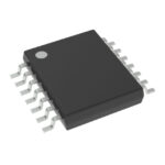 SN74LVC7001APWRQ1
Choose LED drivers by current, string voltage, dimming and thermal limits. Understand constant-current operation and the checks needed for your load.
Read More
SN74LVC7001APWRQ1 is listed in the Inverter Gates range at ChipApex. The manufacturer field lists Texas Instruments. Its product description is AUTOMOTIVE QUADRUPLE TWO-INPUT 1.…
Read More
SN74LVC7001APWRQ1 is listed in the Inverter Gates range at ChipApex. The manufacturer field lists Texas Instruments. Its product description is AUTOMOTIVE QUADRUPLE TWO-INPUT 1.…
Read More
SN74LVC7001APWRQ1 is listed in the Inverter Gates range at ChipApex. The manufacturer field lists Texas Instruments. Its product description is AUTOMOTIVE QUADRUPLE TWO-INPUT 1.…
Read More
Learn how a pressure transducer converts pressure into voltage, current, or digital output, and compare pressure references and key selection specs.
Read More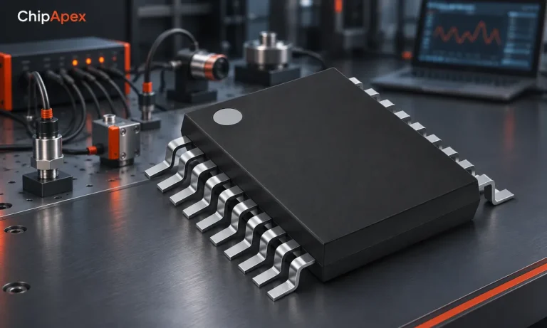
Learn what data acquisition means, from sensors and conditioning to sampling and storage. Review channel timing, wiring, calibration and data quality.
Read More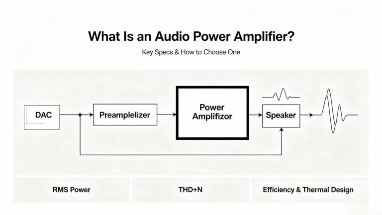
SN74LVC7001APWRQ1 is listed in the Inverter Gates range at ChipApex. The manufacturer field lists Texas Instruments. Its product description is AUTOMOTIVE QUADRUPLE TWO-INPUT 1.…
Read More
SN74LVC7001APWRQ1 is listed in the Inverter Gates range at ChipApex. The manufacturer field lists Texas Instruments. Its product description is AUTOMOTIVE QUADRUPLE TWO-INPUT 1.…
Read More
SN74LVC7001APWRQ1 is listed in the Inverter Gates range at ChipApex. The manufacturer field lists Texas Instruments. Its product description is AUTOMOTIVE QUADRUPLE TWO-INPUT 1.…
Read More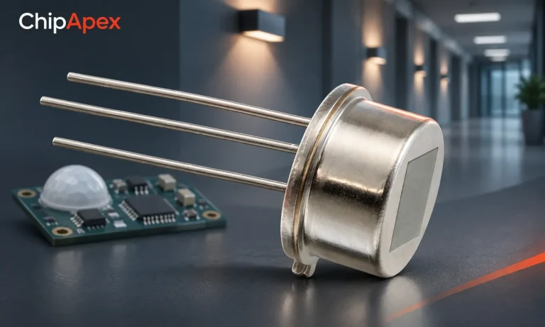
Understand how motion sensors work. Compare PIR, radar and ultrasonic sensing, then check presence detection, false triggers, optics and signal conditioning.
Read More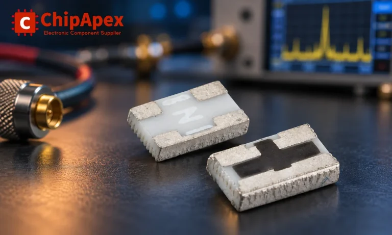
Understand RF attenuator dB values, fixed and programmable types, impedance, power limits and noise tradeoffs before choosing parts for an RF signal path.
Read More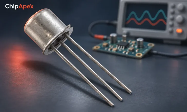
Learn what a transistor does in a circuit. Compare switching and amplification, BJT and MOSFET drive, operating limits and practical component selection.
Read More
The activity of extra discounts on wholesale prices is in full swing…
Please fill in your contact information and we will send you the latest wholesale price list.





