 ChipApex | Global Electronic Components Supplier

SEARCH
Search Product
Search Post
— IC芯片 | 连接器 | 传感器 | 被动器件 —
Search productSearch post
— IC芯片 | 连接器 | 传感器 | 被动器件 —
Consult the customer manager about the wholesale price.
consultation hotline:86-132-6715-2157
email:[email protected]
Contact the product manager for consultation. One-stop consultation is available.
Do you want a lower wholesale price? Please send us your inquiry and we will reply immediately.
SN74SSTU32866ZKER is listed in the Specialty Logic range at ChipApex. The manufacturer field lists Texas Instruments. Its product description is IC 25BIT CONFIG REG BUFF 96-BGA. Review the specifications below when checking this part for your BOM.
The SN74SSTU32866GKER is a Widebus+ registered buffer designed for DDR2 DIMM applications. It operates at VCC = 1.7V to 1.9V and accepts SSTL_18 data inputs with LVCMOS control signals. The device supports differential clock inputs (CLK, CLK) and registers data on the rising edge of CLK and falling edge of CLK. It features configurable pinouts: 25-bit 1:1 or 14-bit 1:2 (Register A/B). It includes parity checking on DIMM-independent data inputs, outputting errors via an open-drain QERR pin. Chip-select inputs (DCS, CSR) gate outputs to minimize power consumption.
Verify the specific ordering suffix GKER corresponds to the tape and reel packaging variant. Confirm the component meets RoHS compliance standards required for your assembly process. Ensure the design accommodates the LFBGA package thermal characteristics and pinout configuration selected via C0 and C1 hard-wired inputs.
Select this component when designing DDR2 memory interfaces requiring wide bus width buffering with integrated parity checking. Choose the 1:1 configuration for single-device driving or 1:2 for dual-device cascading. Ensure the system provides stable differential clocks and appropriate SSTL_18 termination voltages for reliable signal integrity.
Part of Texas Instruments' Widebus+ family, optimized for high-density memory modules. The SN74SSTU32866 addresses the need for robust data registration and error detection in modern server memory designs, replacing older discrete logic solutions with a highly integrated buffered approach.
No public confirmed substitute part numbers are documented in the provided datasheet.
The device checks parity on DIMM-independent data inputs. If an error occurs, the open-drain QERR output is driven low and latched for a minimum of two clock cycles or until RESET is asserted.
C0 and C1 are hard-wired configuration inputs that select between the 25-bit 1:1 mode and the 14-bit 1:2 Register A or Register B pinout configurations. They should not be switched during normal operation.
Explore related parts through Logic, Integrated Circuits (ICs), all product categories, ChipApex homepage.
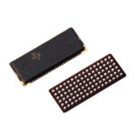 SN74SSTU32866ZKER
 is listed in the Specialty Logic range at ChipApex. The manufacturer field lists Texas Instruments. Its product description is IC 25BIT CONFIG REG…
Read More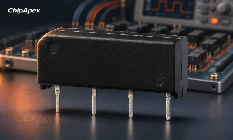
Choose a reed relay for signal switching. Understand hot and cold switching, leakage, contact resistance, isolation and measurement settling requirements.
Read More
SN74SSTU32866ZKER is listed in the Specialty Logic range at ChipApex. The manufacturer field lists Texas Instruments. Its product description is IC 25BIT CONFIG REG…
Read More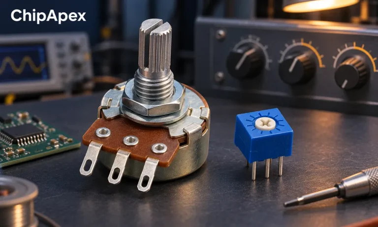
Compare rheostat and potentiometer wiring and functions. Understand divider loading, wiper current, track power and practical component selection.
Read More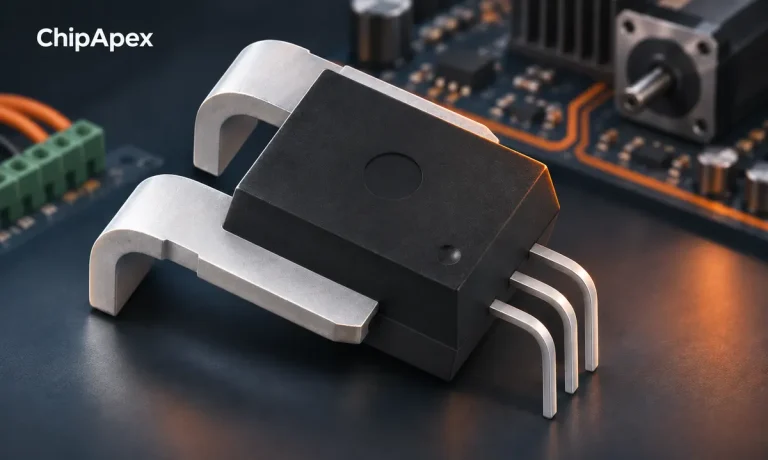
Compare Hall, shunt, current transformer and Rogowski sensing. Check AC/DC capability, accuracy, isolation, heat and response before selecting a sensor.
Read More
SN74SSTU32866ZKER is listed in the Specialty Logic range at ChipApex. The manufacturer field lists Texas Instruments. Its product description is IC 25BIT CONFIG REG…
Read More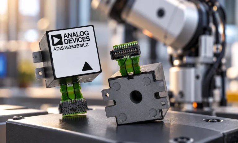
Learn what an IMU measures, how accelerometers and gyroscopes work together, why orientation estimates drift, and what to compare.
Read More
SN74SSTU32866ZKER is listed in the Specialty Logic range at ChipApex. The manufacturer field lists Texas Instruments. Its product description is IC 25BIT CONFIG REG…
Read More
SN74SSTU32866ZKER is listed in the Specialty Logic range at ChipApex. The manufacturer field lists Texas Instruments. Its product description is IC 25BIT CONFIG REG…
Read More
SN74SSTU32866ZKER is listed in the Specialty Logic range at ChipApex. The manufacturer field lists Texas Instruments. Its product description is IC 25BIT CONFIG REG…
Read More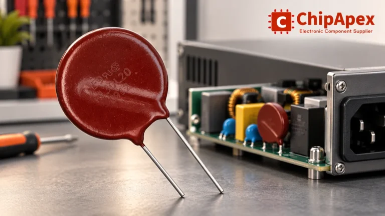
Select MOV varistors by continuous voltage, clamping behavior, surge waveform and repetition. Check thermal disconnection, fuse coordination and replacements.
Read More
SN74SSTU32866ZKER is listed in the Specialty Logic range at ChipApex. The manufacturer field lists Texas Instruments. Its product description is IC 25BIT CONFIG REG…
Read More
The activity of extra discounts on wholesale prices is in full swing…
Please fill in your contact information and we will send you the latest wholesale price list.





