 ChipApex | Global Electronic Components Supplier

SEARCH
Search Product
Search Post
— IC芯片 | 连接器 | 传感器 | 被动器件 —
Search productSearch post
— IC芯片 | 连接器 | 传感器 | 被动器件 —
Consult the customer manager about the wholesale price.
consultation hotline:86-132-6715-2157
email:[email protected]
Contact the product manager for consultation. One-stop consultation is available.
Do you want a lower wholesale price? Please send us your inquiry and we will reply immediately.
SN74V283-7PZA is listed in the FIFOs Memory range at ChipApex. The manufacturer field lists Texas Instruments. Its product description is IC FIFO SYNC 64KX9 5NS 80LQFP. Review the specifications below when checking this part for your BOM.
The SN74V283 is a 3.3-V CMOS first-in, first-out (FIFO) memory with a capacity of 32768 × 18 bits or 65536 × 9 bits. It operates at frequencies up to 166 MHz with a 6-ns read/write cycle time. The device features user-selectable input and output bus widths (×9 or ×18), big-endian/little-endian byte representation, and 5-V tolerant inputs. It supports independent read and write clocks, zero-latency retransmit, and programmable almost-empty/full flags.
Verify the specific ordering suffix matches the required package type, as the SN74V283 family is available in multiple configurations. Confirm that the selected variant aligns with the intended memory organization and pinout requirements for your design. Ensure compatibility with 3.3-V logic levels and check for any specific environmental or reliability certifications required by your application standards before finalizing procurement.
Select the SN74V283 when deep memory depth combined with high-speed operation is necessary. Choose this component if your design requires independent read and write clocks or flexible bus width matching between ×9 and ×18 systems. Consider this part for applications demanding precise control over data latency through programmable flags and retransmit functions.
The SN74V283 belongs to the Texas Instruments SN74V series of high-speed CMOS FIFO memories. This series includes variants like the SN74V263, SN74V273, and SN74V293, which differ primarily in memory depth. The SN74V283 specifically offers 32768 × 18 or 65536 × 9 bit capacities, positioning it between the smaller SN74V273 and the larger SN74V293 in terms of storage capability within the same functional family.
SN74V273PZA
In FWFT mode, the first word written to an empty FIFO appears on the outputs after three RCLK cycles without requiring the Read Enable (REN) signal to be asserted. Subsequent words require REN to be low for access.
Asserting the RT pin low during a rising RCLK edge resets the read pointer to the first location of the memory array, allowing data to be reread from the beginning without disturbing the write pointer or other settings.
Yes, the SN74V283 supports flexible bus matching. The input width (IW) and output width (OW) can be configured independently to be either ×9 or ×18, allowing for conversions such as ×18 input to ×9 output.
Explore related parts through Logic, Integrated Circuits (ICs), all product categories, ChipApex homepage.
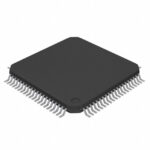 SN74V283-7PZA

SN74V283-7PZA is listed in the FIFOs Memory range at ChipApex. The manufacturer field lists Texas Instruments. Its product description is IC FIFO SYNC 64KX9…
Read More
SN74V283-7PZA is listed in the FIFOs Memory range at ChipApex. The manufacturer field lists Texas Instruments. Its product description is IC FIFO SYNC 64KX9…
Read More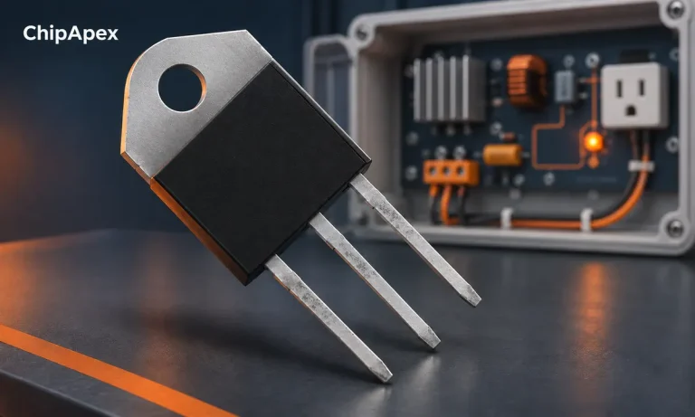
Learn how a TRIAC switches AC loads. Understand triggering, latching, holding current, phase control and thermal limits before choosing a component.
Read MoreSN74V283-7PZA is listed in the FIFOs Memory range at ChipApex. The manufacturer field lists Texas Instruments. Its product description is IC FIFO SYNC 64KX9…
Read More
SN74V283-7PZA is listed in the FIFOs Memory range at ChipApex. The manufacturer field lists Texas Instruments. Its product description is IC FIFO SYNC 64KX9…
Read More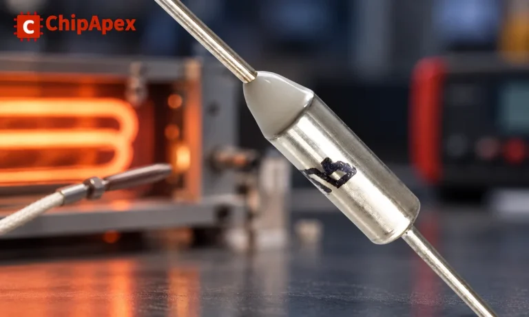
Understand thermal fuse operation, Tf, Th and Tm, electrical ratings and mounting. Check temperature limits and replacement requirements for your design.
Read More
SN74V283-7PZA is listed in the FIFOs Memory range at ChipApex. The manufacturer field lists Texas Instruments. Its product description is IC FIFO SYNC 64KX9…
Read More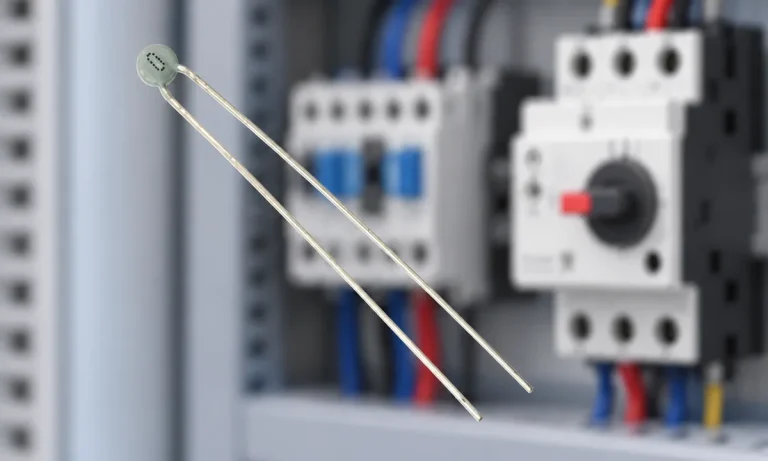
Learn why PTC resistance rises with temperature, how it differs from NTC, and which ratings matter for sensing and protection.
Read More
SN74V283-7PZA is listed in the FIFOs Memory range at ChipApex. The manufacturer field lists Texas Instruments. Its product description is IC FIFO SYNC 64KX9…
Read More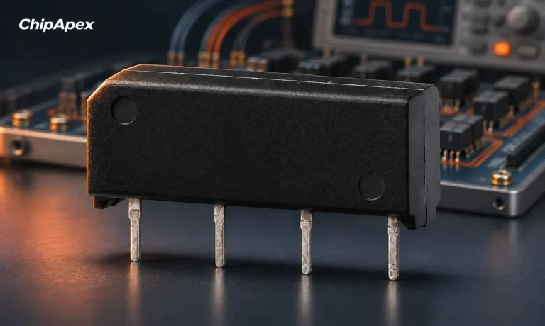
Choose a reed relay for signal switching. Understand hot and cold switching, leakage, contact resistance, isolation and measurement settling requirements.
Read More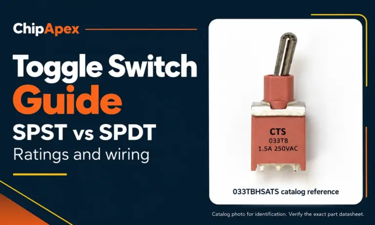
Compare SPST and SPDT toggle switches, understand AC/DC ratings, and follow wiring examples. Check contact action, mounting and parts in the ChipApex catalog.
Read More
SN74V283-7PZA is listed in the FIFOs Memory range at ChipApex. The manufacturer field lists Texas Instruments. Its product description is IC FIFO SYNC 64KX9…
Read More
The activity of extra discounts on wholesale prices is in full swing…
Please fill in your contact information and we will send you the latest wholesale price list.





