 ChipApex | Global Electronic Components Supplier

SEARCH
Search Product
Search Post
— IC芯片 | 连接器 | 传感器 | 被动器件 —
Search productSearch post
— IC芯片 | 连接器 | 传感器 | 被动器件 —
Consult the customer manager about the wholesale price.
consultation hotline:86-132-6715-2157
email:[email protected]
Contact the product manager for consultation. One-stop consultation is available.
Do you want a lower wholesale price? Please send us your inquiry and we will reply immediately.
SY89871UMG-TR is listed in the Clock Buffers, Drivers range at ChipApex. The manufacturer field lists Microchip Technology. Its product description is IC CLK BUFFER 1:3 2.5GHZ 16MLF. Review the specifications below when checking this part for your BOM.
The SY89871UMG-TR is a programmable clock divider and fanout buffer featuring LVPECL outputs. It accepts high-speed differential inputs (CML, LVDS, PECL, HSTL) via an internal termination network accessible through the VT pin. The device provides two phase-matched output banks: Bank A passes the input frequency undivided, while Bank B divides the frequency by 2, 4, 8, or 16 based on parallel programming pins. It operates on a 2.375V to 3.6V supply with a maximum toggle frequency of 2.5GHz and supports AC or DC coupling.
Verify that the ordering suffix 'TR' corresponds to the tape and reel packaging variant as specified in the datasheet. Confirm the package type is QFN-16 and check for the Pb-Free bar line indicator marking. Ensure the operating temperature range meets industrial requirements (-40°C to +85°C).
Select this component when a single-ended or differential clock source requires division into multiple lower-frequency signals with precise phase matching. The VT pin allows adaptation to various logic standards without external termination components. Verify that the required divider ratio matches the available S1/S0 pin configurations.
This part belongs to the Precision Edge family of clock dividers and buffers. It serves as a solution for distributing and dividing high-speed clock signals in telecommunications infrastructure. The device integrates both the divider function and the fanout buffer into a single 16-pin QFN package.
The SY89874U is a related product offering similar functionality but includes a 1:2 fanout buffer in addition to the programmable divider. Verify if the additional fanout capability is required for the specific application layout.
The device features internal 50Ω termination resistors connected to the VT pin. For CML and LVDS inputs, the VT pin should be left floating.
The divider ratios are 2, 4, 8, and 16, selected via the S1 and S0 parallel programming pins.
Yes, the device includes a VREF-AC reference voltage (approx. VCC–1.4V) specifically designed for AC-coupled applications.
Explore related parts through Clock/Timing, Integrated Circuits (ICs), all product categories, ChipApex homepage.
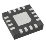 SY89871UMG-TR
Learn how a pressure transducer converts pressure into voltage, current, or digital output, and compare pressure references and key selection specs.
Read More
SY89871UMG-TR is listed in the Clock Buffers, Drivers range at ChipApex. The manufacturer field lists Microchip Technology. Its product description is IC CLK BUFFER…
Read More
SY89871UMG-TR is listed in the Clock Buffers, Drivers range at ChipApex. The manufacturer field lists Microchip Technology. Its product description is IC CLK BUFFER…
Read More
Select a bridge rectifier by reverse voltage, capacitor charging current, startup surge and cooling. Work through a stated DC voltage and ripple example.
Read More
SY89871UMG-TR is listed in the Clock Buffers, Drivers range at ChipApex. The manufacturer field lists Microchip Technology. Its product description is IC CLK BUFFER…
Read More
SY89871UMG-TR is listed in the Clock Buffers, Drivers range at ChipApex. The manufacturer field lists Microchip Technology. Its product description is IC CLK BUFFER…
Read More
SY89871UMG-TR is listed in the Clock Buffers, Drivers range at ChipApex. The manufacturer field lists Microchip Technology. Its product description is IC CLK BUFFER…
Read More
Choose a DIP switch by contact type, coded positions, footprint and signal ratings. Check logic polarity, assembly conditions and PCB configuration behavior.
Read More
See when an inductor behaves linearly, how DC bias and saturation reduce inductance, and which current and temperature curves to check.
Read More
SY89871UMG-TR is listed in the Clock Buffers, Drivers range at ChipApex. The manufacturer field lists Microchip Technology. Its product description is IC CLK BUFFER…
Read More
Understand how a comparator switches at a voltage threshold, why hysteresis prevents chatter, and which output and input specs matter.
Read More
SY89871UMG-TR is listed in the Clock Buffers, Drivers range at ChipApex. The manufacturer field lists Microchip Technology. Its product description is IC CLK BUFFER…
Read More
The activity of extra discounts on wholesale prices is in full swing…
Please fill in your contact information and we will send you the latest wholesale price list.






