 ChipApex | Global Electronic Components Supplier

SEARCH
Search Product
Search Post
— IC芯片 | 连接器 | 传感器 | 被动器件 —
Search productSearch post
— IC芯片 | 连接器 | 传感器 | 被动器件 —
Consult the customer manager about the wholesale price.
consultation hotline:86-132-6715-2157
email:[email protected]
Contact the product manager for consultation. One-stop consultation is available.
Do you want a lower wholesale price? Please send us your inquiry and we will reply immediately.
TC7SP3125TU,LF is listed in the Translators, Level Shifters range at ChipApex. The manufacturer field lists Toshiba Semiconductor and Storage. Its product description is IC TRANSLTR UNIDIRECTIONAL UF6. Review the specifications below when checking this part for your BOM.
The TC7SP3125TU is a low-voltage, low-power 1-bit dual-supply bus buffer fabricated with advanced high-speed CMOS technology. It interfaces between a 1.2 V to 2.5 V A-bus and a 1.8 V to 3.3 V B-bus. The device features overvoltage tolerant inputs and outputs up to 3.6 V, power-down protection, and an enable input (OE) for signal isolation. Propagation delay ranges from 6.8 ns at VCCA=2.5V/VCCB=3.3V to 30 ns at VCCA=1.2V/VCCB=1.8V. Output current capability is 12 mA min at VCCB=3.0V. Operating temperature range is -40°C to 85°C.
Verify the specific ordering suffix matches the required tape-and-reel quantity and marking configuration. Confirm RoHS compliance status and environmental declarations with the manufacturer prior to procurement. Ensure the UF6 package dimensions align with the target PCB footprint constraints.
Select this component for applications requiring bidirectional data transfer between disparate voltage domains. Evaluate propagation delay specifications against the system clock requirements for the specific VCCA and VCCB operating points. Consider the ultra-small UF6 package size if board space is limited in portable electronics designs.
This part belongs to Toshiba's TC7SP series of low-voltage CMOS digital integrated circuits. It functions specifically as a single-bit bus transceiver designed for voltage translation. The UF6 package provides a compact solution compared to standard small-outline packages, targeting space-constrained mobile and handheld electronic devices.
Check for pin-compatible alternatives within the same Toshiba family that may offer updated packaging or revised electrical characteristics. Verify that any substitute maintains the same dual-supply voltage tolerance and overvoltage protection ratings.
No. Unused inputs and bus inputs must be tied to either VCC or GND to ensure normal operation.
All inputs and outputs are designed with overvoltage tolerance up to 3.6 V.
Explore related parts through Logic, Integrated Circuits (ICs), all product categories, ChipApex homepage.
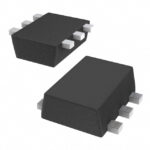 TC7SP3125TU,LF
Learn how a pressure transducer converts pressure into voltage, current, or digital output, and compare pressure references and key selection specs.
Read More
Select a bridge rectifier by reverse voltage, capacitor charging current, startup surge and cooling. Work through a stated DC voltage and ripple example.
Read More
TC7SP3125TU,LF is listed in the Translators, Level Shifters range at ChipApex. The manufacturer field lists Toshiba Semiconductor and Storage. Its product description is IC…
Read More
TC7SP3125TU,LF is listed in the Translators, Level Shifters range at ChipApex. The manufacturer field lists Toshiba Semiconductor and Storage. Its product description is IC…
Read More
See how a MEMS gyroscope measures angular rate, why its angle estimate drifts, and which range, noise, interface and temperature specs to compare.
Read More
TC7SP3125TU,LF is listed in the Translators, Level Shifters range at ChipApex. The manufacturer field lists Toshiba Semiconductor and Storage. Its product description is IC…
Read More
TC7SP3125TU,LF is listed in the Translators, Level Shifters range at ChipApex. The manufacturer field lists Toshiba Semiconductor and Storage. Its product description is IC…
Read More
Choose an AC to DC converter by input range, output demand, isolation, efficiency and thermal derating. Compare architectures and check installation needs.
Read More
Learn what an IMU measures, how accelerometers and gyroscopes work together, why orientation estimates drift, and what to compare.
Read More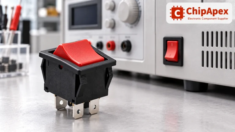
Choose a rocker switch by AC/DC ratings, contact arrangement, illumination, panel fit and sealing. Get practical checks for engineering and component sourcing.
Read More
TC7SP3125TU,LF is listed in the Translators, Level Shifters range at ChipApex. The manufacturer field lists Toshiba Semiconductor and Storage. Its product description is IC…
Read More
TC7SP3125TU,LF is listed in the Translators, Level Shifters range at ChipApex. The manufacturer field lists Toshiba Semiconductor and Storage. Its product description is IC…
Read More
The activity of extra discounts on wholesale prices is in full swing…
Please fill in your contact information and we will send you the latest wholesale price list.





