 ChipApex | Global Electronic Components Supplier

SEARCH
Search Product
Search Post
— IC芯片 | 连接器 | 传感器 | 被动器件 —
Search productSearch post
— IC芯片 | 连接器 | 传感器 | 被动器件 —
Consult the customer manager about the wholesale price.
consultation hotline:86-132-6715-2157
email:[email protected]
Contact the product manager for consultation. One-stop consultation is available.
Do you want a lower wholesale price? Please send us your inquiry and we will reply immediately.
XCV1000E-8FG680C is listed in the Field Programmable Gate Array range at ChipApex. The manufacturer field lists AMD. Its product description is IC FPGA 512 I/O 680FTEBGA. Review the specifications below when checking this part for your BOM.
The XCV1000E-8FG680C is a Virtex-E Field Programmable Gate Array manufactured by AMD (formerly Xilinx). It utilizes a 0.18 µm CMOS process with a 1.8 V core voltage and operates within the commercial temperature range of 0°C to +85°C. The device features 331,776 system gates, 27,648 logic cells, and 6,144 Configurable Logic Blocks (CLBs). It includes 393,216 bits of Block SelectRAM and 393,216 bits of distributed RAM. The FG680 package provides up to 512 user I/Os and supports high-speed differential signaling standards.
Verify component authenticity through authorized distributors or official manufacturer channels. Confirm RoHS compliance status as early production runs may vary. Ensure proper ESD handling procedures are followed during storage and installation. Validate that the specific speed grade (-8) meets the target timing requirements for the intended design application.
Select this model when designs require high-density logic resources combined with substantial embedded memory capacity. The -8 speed grade offers specific timing characteristics suitable for moderate-frequency synchronous applications. Consider the 1.8 V core voltage requirements and ensure adequate power delivery network design for the associated I/O supply voltages.
This component belongs to the Virtex-E family, representing an evolutionary step from the original Virtex series. It offers increased performance and lower power consumption due to the advanced 0.18 µm process technology. The architecture maintains pin compatibility with certain Virtex packages while introducing enhanced I/O flexibility and additional DLL resources.
The XCV1000E-6FG680C serves as a faster alternative within the same package and family. Designers migrating from the standard Virtex XCV1000 must account for architectural differences and recompile their bitstreams, as the devices are not bitstream-compatible despite physical similarities.
Virtex-E devices utilize a 0.18 µm process with a 1.8 V core voltage, offering up to 30% higher performance than the 2.5 V Virtex family. They also feature eight DLLs compared to four in Virtex devices and support additional I/O standards like LVPECL.
According to the Virtex-E Family Maximum User I/O table, the FG680 package supports up to 512 user I/Os for the XCV1000E device.
Yes, in Virtex-E devices, input buffers for LVTTL, LVCMOS2, and PCI standards are supplied by the I/O supply voltage VCCO rather than the internal VCCINT, allowing mixing of input and output buffers with the same VCCO.
Explore related parts through Embedded, Integrated Circuits (ICs), all product categories, ChipApex homepage.
 XCV1000E-8FG680C
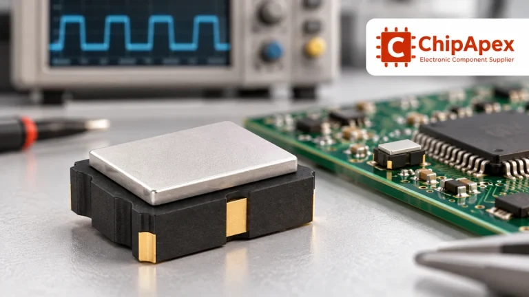
Compare RC, crystal and MEMS oscillator circuits. Check ppm, jitter, load capacitance, startup margin and output compatibility before choosing a clock source.
Read More
XCV1000E-8FG680C is listed in the Field Programmable Gate Array range at ChipApex. The manufacturer field lists AMD. Its product description is IC FPGA 512…
Read More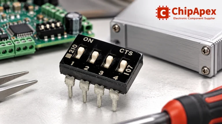
Choose a DIP switch by contact type, coded positions, footprint and signal ratings. Check logic polarity, assembly conditions and PCB configuration behavior.
Read More
XCV1000E-8FG680C is listed in the Field Programmable Gate Array range at ChipApex. The manufacturer field lists AMD. Its product description is IC FPGA 512…
Read More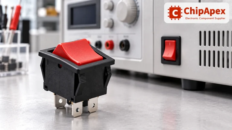
Choose a rocker switch by AC/DC ratings, contact arrangement, illumination, panel fit and sealing. Get practical checks for engineering and component sourcing.
Read More
XCV1000E-8FG680C is listed in the Field Programmable Gate Array range at ChipApex. The manufacturer field lists AMD. Its product description is IC FPGA 512…
Read More
XCV1000E-8FG680C is listed in the Field Programmable Gate Array range at ChipApex. The manufacturer field lists AMD. Its product description is IC FPGA 512…
Read More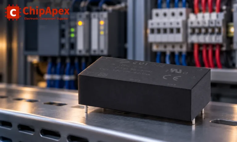
Choose an AC to DC converter by input range, output demand, isolation, efficiency and thermal derating. Compare architectures and check installation needs.
Read More
XCV1000E-8FG680C is listed in the Field Programmable Gate Array range at ChipApex. The manufacturer field lists AMD. Its product description is IC FPGA 512…
Read More
XCV1000E-8FG680C is listed in the Field Programmable Gate Array range at ChipApex. The manufacturer field lists AMD. Its product description is IC FPGA 512…
Read More
Understand how a comparator switches at a voltage threshold, why hysteresis prevents chatter, and which output and input specs matter.
Read More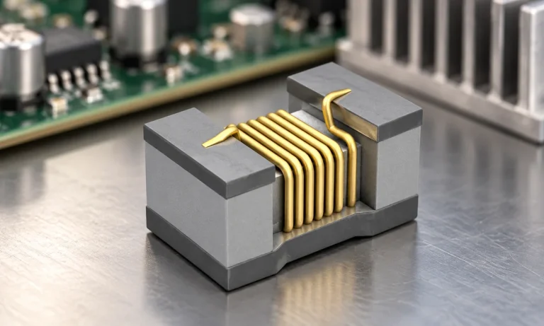
See when an inductor behaves linearly, how DC bias and saturation reduce inductance, and which current and temperature curves to check.
Read More
The activity of extra discounts on wholesale prices is in full swing…
Please fill in your contact information and we will send you the latest wholesale price list.






