 ChipApex | Global Electronic Components Supplier

SEARCH
Search Product
Search Post
— IC芯片 | 连接器 | 传感器 | 被动器件 —
Search productSearch post
— IC芯片 | 连接器 | 传感器 | 被动器件 —
Consult the customer manager about the wholesale price.
consultation hotline:86-132-6715-2157
email:[email protected]
Contact the product manager for consultation. One-stop consultation is available.
Do you want a lower wholesale price? Please send us your inquiry and we will reply immediately.
XCV600-4FG676C is listed in the Field Programmable Gate Array range at ChipApex. The manufacturer field lists AMD. Its product description is IC FPGA 444 I/O 676FCBGA. Review the specifications below when checking this part for your BOM.
The XCV600-4FGG676C is a Virtex FPGA featuring 661,111 system gates and 15,552 logic cells within a 48x72 CLB array. It operates at a maximum clock frequency of 200 MHz with a -4 speed grade. The device utilizes a 0.22 μm process and supports up to 444 user I/Os in the FG676 package. It includes 98,304 bits of Block SelectRAM and four DLLs for clock management.
This component is officially listed as obsolete under Xilinx Notice XCN10016. Verification of current availability requires consulting authorized distributors for end-of-life status. Designers should confirm if the part remains in production or has reached final shipment dates before initiating procurement processes.
Select this model for designs requiring approximately 660k system gates and 200 MHz performance. Ensure the FG676 package fits the PCB footprint. Verify that the 2.5V core voltage and specific I/O bank requirements align with the target system power rails and signaling standards.
The XCV600 belongs to the original Virtex family, representing a significant advancement in silicon efficiency through its 0.22 μm five-layer metal CMOS process. It serves as a high-capacity alternative to mask-programmed gate arrays, offering extensive routing resources and advanced clock distribution networks.
As an obsolete product, direct replacements are not specified in the datasheet. Review Xilinx notice XCN10016 for guidance on transitioning to newer FPGA families or alternative components that match the required gate count and performance specifications.
Explore related parts through Embedded, Integrated Circuits (ICs), all product categories, ChipApex homepage.
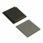 XCV600-4FG676C

XCV600-4FG676C is listed in the Field Programmable Gate Array range at ChipApex. The manufacturer field lists AMD. Its product description is IC FPGA 444…
Read More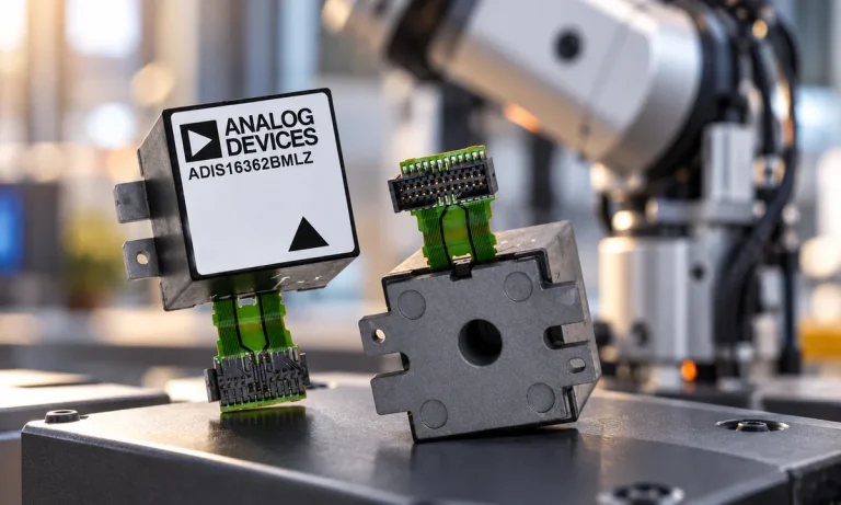
Learn what an IMU measures, how accelerometers and gyroscopes work together, why orientation estimates drift, and what to compare.
Read More
XCV600-4FG676C is listed in the Field Programmable Gate Array range at ChipApex. The manufacturer field lists AMD. Its product description is IC FPGA 444…
Read More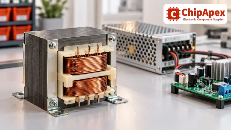
Select power transformers by input frequency, secondary VA, rectifier load, isolation, regulation and inrush. Build a clearer specification for your next RFQ.
Read More
XCV600-4FG676C is listed in the Field Programmable Gate Array range at ChipApex. The manufacturer field lists AMD. Its product description is IC FPGA 444…
Read More
XCV600-4FG676C is listed in the Field Programmable Gate Array range at ChipApex. The manufacturer field lists AMD. Its product description is IC FPGA 444…
Read More
Learn why PTC resistance rises with temperature, how it differs from NTC, and which ratings matter for sensing and protection.
Read More
Learn how an analog front end conditions sensor signals. Compare gain, noise, filtering, ADC settling and integration options before selecting components.
Read MoreXCV600-4FG676C is listed in the Field Programmable Gate Array range at ChipApex. The manufacturer field lists AMD. Its product description is IC FPGA 444…
Read More
XCV600-4FG676C is listed in the Field Programmable Gate Array range at ChipApex. The manufacturer field lists AMD. Its product description is IC FPGA 444…
Read More
XCV600-4FG676C is listed in the Field Programmable Gate Array range at ChipApex. The manufacturer field lists AMD. Its product description is IC FPGA 444…
Read More
XCV600-4FG676C is listed in the Field Programmable Gate Array range at ChipApex. The manufacturer field lists AMD. Its product description is IC FPGA 444…
Read More
The activity of extra discounts on wholesale prices is in full swing…
Please fill in your contact information and we will send you the latest wholesale price list.






