 ChipApex | Global Electronic Components Supplier
5SGXMA5N3F45I3N
Search Product
Search Post
— IC芯片 | 连接器 | 传感器 | 被动器件 —
Search productSearch post
— IC芯片 | 连接器 | 传感器 | 被动器件 —
Consult the customer manager about the wholesale price.
consultation hotline:86-132-6715-2157
email:[email protected]
Contact the product manager for consultation. One-stop consultation is available.
Do you want a lower wholesale price? Please send us your inquiry and we will reply immediately.
The Altera 5SGXMA5N3F45I3N is a Stratix V GX Field Programmable Gate Array (FPGA) designed for high-performance digital signal processing and networking applications. It features 2640 Logic Array Blocks (LABs), providing substantial logic capacity within the Stratix V architecture. The device integrates 48 high-speed transceivers capable of data rates up to 14.1 Gb/s, supporting advanced serial communication protocols. With 840 I/O pins available in an FCBGA-1932 package, it offers extensive connectivity options. The FPGA includes significant embedded memory resources, totaling approximately 52 Mbit, to support complex data buffering and storage requirements.
Verify component authenticity through authorized channels due to potential availability constraints. Confirm RoHS compliance status and moisture sensitivity level prior to assembly. Ensure proper ESD handling procedures are followed during storage and installation. Check for specific ordering suffixes that may affect pinout or electrical characteristics. Validate lead times as production schedules can vary significantly for legacy components.
Compare against other Stratix V GX variants based on required LAB count and transceiver density. Evaluate power consumption profiles at target operating frequencies. Assess thermal management solutions given the high pin count and performance capabilities. Consider compatibility with Quartus Prime design software versions. Verify package dimensions and footprint against PCB layout constraints.
This component belongs to the Altera Stratix V GX family, which targets high-performance computing and communications markets. The 'GX' designation indicates the inclusion of high-speed transceivers essential for serial data transmission. It sits alongside other Stratix V models differentiated by logic density and I/O configurations. The part represents a mature technology node suitable for established high-end designs.
Direct replacements may be limited due to the specific combination of LABs and transceivers. Consider Stratix V GX devices with similar pin counts but different logic densities if flexibility exists. Evaluate newer Agilex families for future-proofing, though pinouts will differ. Consult official substitution guides for electrically compatible alternatives within the same package type.

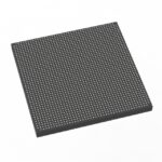 5SGXMA5N3F45I3N
The activity of extra discounts on wholesale prices is in full swing…
Please fill in your contact information and we will send you the latest wholesale price list.




