 ChipApex | Global Electronic Components Supplier
9DBL0242CKILF
Search Product
Search Post
— IC芯片 | 连接器 | 传感器 | 被动器件 —
Search productSearch post
— IC芯片 | 连接器 | 传感器 | 被动器件 —
Consult the customer manager about the wholesale price.
consultation hotline:86-132-6715-2157
email:[email protected]
Contact the product manager for consultation. One-stop consultation is available.
Do you want a lower wholesale price? Please send us your inquiry and we will reply immediately.
The 9DBL0242CKILF is a Renesas Electronics clock buffer designed for PCIe applications. It provides two differential outputs using Low Power HCSL (LP-HCSL) signaling, eliminating the need for external termination resistors by integrating 100Ω terminations. The device supports PCIe Gen 1 through Gen 5 architectures, including Common Clock and Independent Reference modes with spread spectrum tolerance. Operating on a single 3.3V supply, it functions within a frequency range of 1 MHz to 200 MHz. The component is housed in a compact 24-VFQFPN package measuring 4 mm x 4 mm, suitable for space-constrained designs.
Verify the specific suffix 'CKILF' against the official Renesas datasheet to confirm package type, lead finish, and RoHS compliance status. Confirm current production status as clock buffer models may transition to end-of-life or be superseded by newer generation devices. Ensure the selected variant matches the required operating temperature range and SMBus configuration options for the target design.
Select this component when a low-pin-count solution is required for fan-out buffering in PCIe systems. The integrated 100Ω termination simplifies PCB layout by removing discrete resistors. Verify that the input signal meets the HCSL voltage levels and that the output drive strength is sufficient for the trace length. Consider the 1-200 MHz frequency range to ensure compatibility with the system's reference clock requirements.
This part belongs to the Renesas 9DBL0x family of PCIe clock buffers. These devices are engineered to support evolving PCIe standards from Gen 1 up to Gen 5/6. The 9DBL0242 variant specifically offers a dual-output configuration, providing a balance between channel count and board space efficiency compared to higher-channel counterparts like the 9DBL04 or 9DBL06 series.
Direct pin-compatible replacements within the same family include the 9DBL0252CKILF, which features integrated 85Ω terminations instead of 100Ω. Designers must verify transmission line impedance requirements before substituting. Other multi-output variants such as the 9DBL0442 or 9DBL0641 offer more channels but require different footprints.
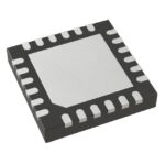 9DBL0242CKILF
The activity of extra discounts on wholesale prices is in full swing…
Please fill in your contact information and we will send you the latest wholesale price list.







