 ChipApex | Global Electronic Components Supplier

SEARCH
Search Product
Search Post
— IC芯片 | 连接器 | 传感器 | 被动器件 —
Search productSearch post
— IC芯片 | 连接器 | 传感器 | 被动器件 —
Consult the customer manager about the wholesale price.
consultation hotline:86-132-6715-2157
email:[email protected]
Contact the product manager for consultation. One-stop consultation is available.
Do you want a lower wholesale price? Please send us your inquiry and we will reply immediately.
ADC12D2000RFIUT/NOPB is listed in the Analog To Digital Converters (ADC) range at ChipApex. The manufacturer field lists Texas Instruments. Its product description is IC ADC 12BIT FOLD INTERP 292BGA. Review the specifications below when checking this part for your BOM.
The ADC12D2000RFIUT/NOPB is a 12-bit, single-channel RF sampling analog-to-digital converter (ADC) from Texas Instruments. It operates at a sampling rate of 4.0 GSPS in interleaved mode or 2.0 GSPS in dual-ADC mode. The device supports direct input frequencies up to and above 2.7 GHz, extending usability beyond the third Nyquist zone. Key electrical specifications include a typical Signal-to-Noise Ratio (SNR) of 54.8 dB, an Effective Number of Bits (ENOB) of 8.7 bits, and a Spurious-Free Dynamic Range (SFDR) of 64.6 dBc at 498 MHz input. Power consumption is typically 4.6 W for the interleaved configuration and 2.3 W per channel in dual mode. The component is housed in a lead-free, thermally enhanced 292-ball BGA package.
Verify the specific ordering suffix against manufacturer documentation to confirm package type and environmental rating. The 'NOPB' suffix indicates a lead-free product. Confirm that the required external components, such as the 3.3 kΩ ±0.1% resistors for Rext and Rtrim terminals, are included in the procurement scope, as they are necessary for achieving rated linearity and input impedance calibration.
Select this component when high-speed RF sampling is required directly at frequencies exceeding 2.7 GHz without intermediate mixing stages. Ensure the design accommodates the 4.6 W power dissipation in interleaved mode through adequate thermal management on the PCB. Verify that the host system can handle the high-speed LVDS output data rates and that the clocking architecture supports the required jitter specifications for the target application bandwidth.
This part belongs to the ADC12D2000RF family of high-speed RF sampling ADCs. It is pin-compatible with other devices in the ADC1xD1x00 and ADC12Dx00RF series, facilitating potential design upgrades or replacements within existing hardware architectures. The device is designed for industrial temperature ranges (-40°C to +85°C) and utilizes a thermally enhanced BGA package to manage heat dissipation effectively.
The datasheet notes pin compatibility with the ADC1xD1x00 and ADC12Dx00RF families. Verify functional equivalence and register compatibility before substituting these parts, as feature sets may vary between specific model numbers within the broader family.
Explore related parts through Data Acquisition, Integrated Circuits (ICs), all product categories, ChipApex homepage.
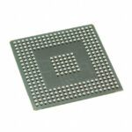 ADC12D2000RFIUT/NOPB

ADC12D2000RFIUT/NOPB is listed in the Analog To Digital Converters (ADC) range at ChipApex. The manufacturer field lists Texas Instruments. Its product description is IC…
Read More
ADC12D2000RFIUT/NOPB is listed in the Analog To Digital Converters (ADC) range at ChipApex. The manufacturer field lists Texas Instruments. Its product description is IC…
Read More
ADC12D2000RFIUT/NOPB is listed in the Analog To Digital Converters (ADC) range at ChipApex. The manufacturer field lists Texas Instruments. Its product description is IC…
Read More
ADC12D2000RFIUT/NOPB is listed in the Analog To Digital Converters (ADC) range at ChipApex. The manufacturer field lists Texas Instruments. Its product description is IC…
Read More
ADC12D2000RFIUT/NOPB is listed in the Analog To Digital Converters (ADC) range at ChipApex. The manufacturer field lists Texas Instruments. Its product description is IC…
Read More
Learn how a pressure transducer converts pressure into voltage, current, or digital output, and compare pressure references and key selection specs.
Read More
Learn what an integrated circuit is, how ICs work, the main types and the specs to check before choosing a part for your design…
Read More
ADC12D2000RFIUT/NOPB is listed in the Analog To Digital Converters (ADC) range at ChipApex. The manufacturer field lists Texas Instruments. Its product description is IC…
Read More
Select a bridge rectifier by reverse voltage, capacitor charging current, startup surge and cooling. Work through a stated DC voltage and ripple example.
Read More
ADC12D2000RFIUT/NOPB is listed in the Analog To Digital Converters (ADC) range at ChipApex. The manufacturer field lists Texas Instruments. Its product description is IC…
Read More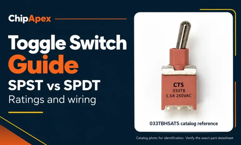
Compare SPST and SPDT toggle switches, understand AC/DC ratings, and follow wiring examples. Check contact action, mounting and parts in the ChipApex catalog.
Read More
Select MOV varistors by continuous voltage, clamping behavior, surge waveform and repetition. Check thermal disconnection, fuse coordination and replacements.
Read More
The activity of extra discounts on wholesale prices is in full swing…
Please fill in your contact information and we will send you the latest wholesale price list.





