 ChipApex | Global Electronic Components Supplier
IDT74FST163244PAG
Search Product
Search Post
— IC芯片 | 连接器 | 传感器 | 被动器件 —
Search productSearch post
— IC芯片 | 连接器 | 传感器 | 被动器件 —
Consult the customer manager about the wholesale price.
consultation hotline:86-132-6715-2157
email:[email protected]
Contact the product manager for consultation. One-stop consultation is available.
Do you want a lower wholesale price? Please send us your inquiry and we will reply immediately.
The IDT74FST163244PAG is a 16-bit bus switch manufactured by Renesas Electronics Corporation. It operates within an industrial temperature range of -40°C to +85°C and requires a supply voltage (VCC) of 5.0V ± 10%. The device features four independent control inputs (xOE) that manage the connection between A and B ports. Key electrical parameters include a typical on-resistance (RON) of 5Ω at VCC = Min. with 12mA current, and a maximum short circuit current of 100mA. Quiescent power supply current is typically 0.1µA, while dynamic power consumption reaches up to 9.4mA during switching. The component utilizes a TSSOP-48 package.
Verify the specific ordering suffix 'PAG' corresponds to the TSSOP-48 Green package variant as defined in the manufacturer's ordering guide. Confirm that the required operating environment falls strictly within the specified industrial temperature range of -40°C to +85°C. Ensure the system design accommodates the 5.0V ± 10% supply voltage requirement to maintain valid logic levels and impedance characteristics.
Select this component when zero propagation delay is critical for signal integrity compared to standard buffers. Consider its pin-compatibility with the FCT16244T if migrating from legacy designs. Evaluate the low quiescent current for power-sensitive applications and verify that the 128mA maximum continuous channel current meets the load requirements of the target circuit.
This device belongs to the FST family of bus switches, designed to connect or isolate ports via n-channel FETs. Unlike traditional logic gates, it provides a bidirectional low-resistance path rather than active driving. The IDT logo indicates its origin from Integrated Device Technology, which has since been acquired by Renesas Electronics.
The datasheet explicitly states the device is functionally similar and pin-compatible with the FCT16244T. Verify that any substitute maintains the same 16-bit flow-through architecture and TSSOP-48 footprint.
The device supports hot insertion because, without VCC applied, the gate-to-source junction of the internal FET is not forward-biased, effectively turning the switch off.
The low on-resistance and direct connection between input and output ports via the n-channel FET reduce the delay in the signal path to close to zero, limited only by the RC delay of the load interacting with the switch.
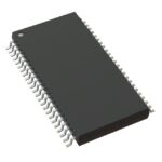 IDT74FST163244PAG
The activity of extra discounts on wholesale prices is in full swing…
Please fill in your contact information and we will send you the latest wholesale price list.






