ChipApex | Global Electronic Components Supplier
LTC2641AIDD-16#PBF
Search Product
Search Post
— IC芯片 | 连接器 | 传感器 | 被动器件 —
Search productSearch post
— IC芯片 | 连接器 | 传感器 | 被动器件 —
Consult the customer manager about the wholesale price.
consultation hotline:86-132-6715-2157
email:[email protected]
Contact the product manager for consultation. One-stop consultation is available.
Do you want a lower wholesale price? Please send us your inquiry and we will reply immediately.
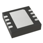
The LTC2641AIDD-16#PBF is a 16-bit unbuffered voltage output digital-to-analog converter (DAC) from Analog Devices. It operates on a single 2.7V to 5.5V supply with a typical current consumption of 120µA. The device features a 3-wire SPI/Microwire compatible serial interface supporting clock rates up to 50MHz. Key electrical specifications include ±1LSB INL and DNL over temperature, a settling time of 1µs to 16 bits, and a glitch impulse of 0.5nV·sec. It is housed in an 8-lead 3mm × 3mm DFN package and functions within an industrial temperature range of –40°C to +85°C.
Verify the specific ordering suffix 'IDD' confirms the industrial temperature grade (–40°C to +85°C) and the 'A' grade for ±1LSB linearity. Confirm the '#PBF' suffix indicates lead-free finish and RoHS compliance. Ensure the DFN-8 package matches the PCB footprint requirements, noting the exposed pad must be soldered to ground.
Select this component for applications requiring high precision (±1LSB) in a compact 3mm × 3mm footprint. The unbuffered output requires loads greater than 60kΩ to maintain linearity; use an external buffer if driving lower impedances. Verify that the system interface supports the 3-wire synchronous protocol and that the reference voltage input range (2V to VDD) aligns with available reference sources.
This part belongs to the LTC2641 family of 16-/14-/12-bit voltage output DACs. The 'A' designation specifies enhanced linearity performance compared to standard grades. The 'IDD' suffix denotes the industrial temperature range and DFN-8 packaging. It serves as a low-power alternative to buffered DACs in space-constrained embedded designs.
Publicly confirmed substitute part numbers are not provided in the source material.
 LTC2641AIDD-16#PBF
The activity of extra discounts on wholesale prices is in full swing…
Please fill in your contact information and we will send you the latest wholesale price list.