 ChipApex | Global Electronic Components Supplier

SEARCH
Search Product
Search Post
— IC芯片 | 连接器 | 传感器 | 被动器件 —
Search productSearch post
— IC芯片 | 连接器 | 传感器 | 被动器件 —
Consult the customer manager about the wholesale price.
consultation hotline:86-132-6715-2157
email:[email protected]
Contact the product manager for consultation. One-stop consultation is available.
Do you want a lower wholesale price? Please send us your inquiry and we will reply immediately.
PI6CBE33045ZHIEX-13R is listed in the Clock Buffers, Drivers range at ChipApex. The manufacturer field lists Diodes Incorporated. Its product description is IC CLK BUFFER 1:4 400MHZ 32TQFN. Review the specifications below when checking this part for your BOM.
The PI6CBE33045 is a low-power, four-output zero-delay buffer (ZDB) and fanout clock buffer designed for PCIe 1.0 through 6.0 and UPI applications. It accepts a differential HCSL input and provides four differential HCSL outputs with integrated 85Ω on-chip termination. The device features a proprietary PLL to achieve very low jitter, supporting selectable bandwidths and spread spectrum tolerance. It operates at a core supply voltage of 3.3V and supports hardware or SMBus control for mode selection and individual output enables.
Verify the ordering suffix 'X' indicates tape and reel packaging and '-13R' specifies top-left corner pin 1 orientation. Confirm the 'I' suffix denotes industrial temperature range (-40°C to +85°C). Ensure the 'E' suffix confirms lead-free and green status. Check current availability as component status may change.
Select this component when driving multiple high-speed serial links requiring low skew and jitter. Use ZDB mode for minimal propagation delay in common-clocked architectures. Use Fanout mode for SRIS architectures. Ensure input clock frequency is within 1-400 MHz. Verify 3.3V supply compatibility and SMBus interface requirements for configuration.
This part belongs to Diodes Incorporated's PI6CBE33xx series of low-power clock buffers. It is specifically optimized for next-generation interconnect standards like PCIe 6.0 and UPI, offering improved jitter performance over previous generations while maintaining compatibility with legacy PCIe standards.
Direct replacements within the same family include PI6CBE3308x and PI6CBE3306x, though these have different output counts and fixed SMBus addresses. Cross-family comparisons should consider output count, package type, and specific jitter specifications for the target application speed.
The device supports an input frequency range from 1 MHz to 400 MHz.
The SMBus address is latched based on the logic levels applied to the SADR0_tri and SADR1_tri pins during startup. For the PI6CBE33045, the base address is D8h, but it can be modified using these tri-level latch pins.
Yes, the PI6CBE33045 is spread spectrum tolerant. It allows for triangular modulation frequencies between 30 kHz and 33 kHz for PCIe applications.
Explore related parts through Clock/Timing, Integrated Circuits (ICs), all product categories, ChipApex homepage.
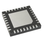 PI6CBE33045ZHIEX-13R

Select a bridge rectifier by reverse voltage, capacitor charging current, startup surge and cooling. Work through a stated DC voltage and ripple example.
Read More
PI6CBE33045ZHIEX-13R is listed in the Clock Buffers, Drivers range at ChipApex. The manufacturer field lists Diodes Incorporated. Its product description is IC CLK BUFFER…
Read More
PI6CBE33045ZHIEX-13R is listed in the Clock Buffers, Drivers range at ChipApex. The manufacturer field lists Diodes Incorporated. Its product description is IC CLK BUFFER…
Read More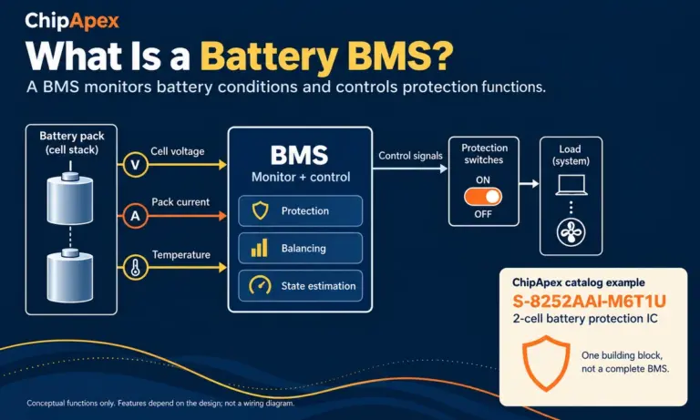
Learn what a battery BMS does, how protection differs from charging, and which pack specifications to check when sourcing BMS components through ChipApex.
Read More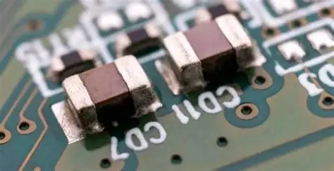
PI6CBE33045ZHIEX-13R is listed in the Clock Buffers, Drivers range at ChipApex. The manufacturer field lists Diodes Incorporated. Its product description is IC CLK BUFFER…
Read More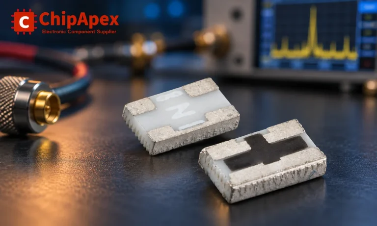
Understand RF attenuator dB values, fixed and programmable types, impedance, power limits and noise tradeoffs before choosing parts for an RF signal path.
Read More
PI6CBE33045ZHIEX-13R is listed in the Clock Buffers, Drivers range at ChipApex. The manufacturer field lists Diodes Incorporated. Its product description is IC CLK BUFFER…
Read More
PI6CBE33045ZHIEX-13R is listed in the Clock Buffers, Drivers range at ChipApex. The manufacturer field lists Diodes Incorporated. Its product description is IC CLK BUFFER…
Read More
PI6CBE33045ZHIEX-13R is listed in the Clock Buffers, Drivers range at ChipApex. The manufacturer field lists Diodes Incorporated. Its product description is IC CLK BUFFER…
Read More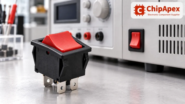
Choose a rocker switch by AC/DC ratings, contact arrangement, illumination, panel fit and sealing. Get practical checks for engineering and component sourcing.
Read More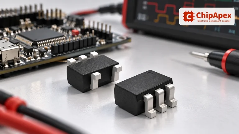
Choose logic inverter ICs by thresholds, supply, output drive and delay. Compare standard and Schmitt-trigger inputs, power sequencing and replacement checks.
Read More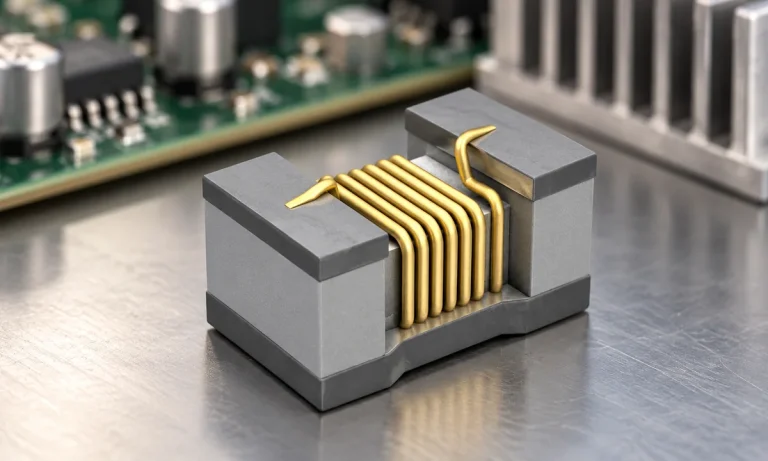
See when an inductor behaves linearly, how DC bias and saturation reduce inductance, and which current and temperature curves to check.
Read More
The activity of extra discounts on wholesale prices is in full swing…
Please fill in your contact information and we will send you the latest wholesale price list.






