 ChipApex | Global Electronic Components Supplier

SEARCH
Search Product
Search Post
— IC芯片 | 连接器 | 传感器 | 被动器件 —
Search productSearch post
— IC芯片 | 连接器 | 传感器 | 被动器件 —
Consult the customer manager about the wholesale price.
consultation hotline:86-132-6715-2157
email:[email protected]
Contact the product manager for consultation. One-stop consultation is available.
Do you want a lower wholesale price? Please send us your inquiry and we will reply immediately.
SN74ALVCH245NSR is listed in the Buffers, Drivers, Receivers, Transceivers range at ChipApex. The manufacturer field lists Texas Instruments. Its product description is IC TXRX NON-INVERT 3.6V 20SO. Review the specifications below when checking this part for your BOM.
The SN74ALVCH245NSR is an octal bus transceiver with 3-state outputs manufactured by Texas Instruments. It operates from a supply voltage range of 1.65 V to 3.6 V and features a maximum propagation delay of 3.4 ns at 3.3 V. The device provides ±24-mA output drive capability at 3.3 V and includes active bus-hold circuitry on data inputs to eliminate the need for external pullup or pulldown resistors. Latch-up performance exceeds 100 mA per JESD 78, Class II standards.
Verify the specific ordering suffix NSR corresponds to the NS package type and tape-and-reel carrier configuration as listed in the official TI ordering information. Confirm that the component meets RoHS compliance requirements and matches the specified operating temperature range of -40°C to 85°C before procurement.
Select this component for designs requiring low-voltage operation between 1.65 V and 3.6 V with high-speed data transfer capabilities. The 3.4 ns propagation delay and ±24-mA drive strength make it suitable for driving moderate loads. Ensure the application utilizes the bus-hold feature to simplify input handling without external resistors.
This part belongs to the SN74ALVCH245 family of octal bus transceivers. It is designed for 1.65-V to 3.6-V VCC operation and is available in multiple package options including SOIC, TSSOP, and TVSOP. The device is intended for bidirectional data transmission controlled by a direction signal.
SN74ALVCH245DW
The device incorporates active bus-hold circuitry on the data inputs, which holds unused or undriven inputs at a valid logic state without requiring external pullup or pulldown resistors.
The output-enable (OE) input disables the device, effectively isolating the buses. To ensure a high-impedance state during power up or power down, OE should be tied to VCC through a pullup resistor.
Explore related parts through Logic, Integrated Circuits (ICs), all product categories, ChipApex homepage.
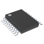 SN74ALVCH245NSR
See how a MEMS gyroscope measures angular rate, why its angle estimate drifts, and which range, noise, interface and temperature specs to compare.
Read More
Learn how a pressure transducer converts pressure into voltage, current, or digital output, and compare pressure references and key selection specs.
Read More
SN74ALVCH245NSR is listed in the Buffers, Drivers, Receivers, Transceivers range at ChipApex. The manufacturer field lists Texas Instruments. Its product description is IC TXRX…
Read More
SN74ALVCH245NSR is listed in the Buffers, Drivers, Receivers, Transceivers range at ChipApex. The manufacturer field lists Texas Instruments. Its product description is IC TXRX…
Read More
Choose a vibration sensor for machine monitoring. Compare sensing methods, bandwidth, noise and mounting, then define the signal-chain requirements.
Read More
Choose an AC to DC converter by input range, output demand, isolation, efficiency and thermal derating. Compare architectures and check installation needs.
Read More
Learn how a JFET works and how to compare bias, leakage, noise and pinout. Review practical selection questions for high-impedance analog circuits.
Read More
SN74ALVCH245NSR is listed in the Buffers, Drivers, Receivers, Transceivers range at ChipApex. The manufacturer field lists Texas Instruments. Its product description is IC TXRX…
Read More
Compare gas sensor technologies, cross-sensitivity and calibration needs. Define the gas, range and environment before choosing a sensing component.
Read More
SN74ALVCH245NSR is listed in the Buffers, Drivers, Receivers, Transceivers range at ChipApex. The manufacturer field lists Texas Instruments. Its product description is IC TXRX…
Read More
SN74ALVCH245NSR is listed in the Buffers, Drivers, Receivers, Transceivers range at ChipApex. The manufacturer field lists Texas Instruments. Its product description is IC TXRX…
Read More
Choose LED drivers by current, string voltage, dimming and thermal limits. Understand constant-current operation and the checks needed for your load.
Read More
The activity of extra discounts on wholesale prices is in full swing…
Please fill in your contact information and we will send you the latest wholesale price list.





