 ChipApex | Global Electronic Components Supplier

SEARCH
Search Product
Search Post
— IC芯片 | 连接器 | 传感器 | 被动器件 —
Search productSearch post
— IC芯片 | 连接器 | 传感器 | 被动器件 —
Consult the customer manager about the wholesale price.
consultation hotline:86-132-6715-2157
email:[email protected]
Contact the product manager for consultation. One-stop consultation is available.
Do you want a lower wholesale price? Please send us your inquiry and we will reply immediately.
SN74HCT165PWR is listed in the Shift Registers range at ChipApex. The manufacturer field lists Texas Instruments. Its product description is 8-BIT PARALLEL-IN/SERIAL-OUT SHI. Review the specifications below when checking this part for your BOM.
The SN74HCT165PWR is an 8-bit parallel-load shift register in a 16-pin TSSOP package. It operates on a 4.5 V to 5.5 V supply with an extended temperature range of –40°C to +125°C. The device features TTL-compatible CMOS inputs and balanced push-pull outputs. Key timing parameters include a maximum propagation delay of 60 ns, a clock frequency up to 25 MHz, and setup/hold times of 25 ns and 9 ns respectively.
Verify the specific ordering suffix 'PW' corresponds to the TSSOP-16 package variant required for your PCB footprint. Confirm that the design supports the specified 4.5 V to 5.5 V operating voltage range. Ensure thermal management aligns with the junction-to-ambient resistance values provided in the datasheet for the target ambient temperature conditions.
Select this component when interfacing with LSTTL or CMOS logic families due to its compatible input thresholds. Choose this part if the application requires an extended industrial temperature range up to +125°C. Consider the balanced push-pull output structure for driving moderate capacitive loads without external buffering.
This device belongs to the Texas Instruments SN74HCT series, which combines high-speed CMOS processing with TTL-compatible input levels. The SN74HCT165 specifically addresses the need for parallel data acquisition in systems where serial communication lines are limited. It serves as a fundamental building block for digital input expansion and data serialization tasks.
SN74HCT165PW
Unused inputs must not be left floating; they should be terminated to either VCC or ground using pull-up or pull-down resistors to prevent undefined operational states and excessive power consumption.
The clock inhibit (CLK INH) input prevents clock pulses from being detected when held high, effectively pausing the shifting operation regardless of the state of the primary clock input.
Explore related parts through Logic, Integrated Circuits (ICs), all product categories, ChipApex homepage.
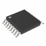 SN74HCT165PWR

SN74HCT165PWR is listed in the Shift Registers range at ChipApex. The manufacturer field lists Texas Instruments. Its product description is 8-BIT PARALLEL-IN/SERIAL-OUT SHI. Review…
Read More
SN74HCT165PWR is listed in the Shift Registers range at ChipApex. The manufacturer field lists Texas Instruments. Its product description is 8-BIT PARALLEL-IN/SERIAL-OUT SHI. Review…
Read More
SN74HCT165PWR is listed in the Shift Registers range at ChipApex. The manufacturer field lists Texas Instruments. Its product description is 8-BIT PARALLEL-IN/SERIAL-OUT SHI. Review…
Read More
SN74HCT165PWR is listed in the Shift Registers range at ChipApex. The manufacturer field lists Texas Instruments. Its product description is 8-BIT PARALLEL-IN/SERIAL-OUT SHI. Review…
Read More
SN74HCT165PWR is listed in the Shift Registers range at ChipApex. The manufacturer field lists Texas Instruments. Its product description is 8-BIT PARALLEL-IN/SERIAL-OUT SHI. Review…
Read More
See how a MEMS gyroscope measures angular rate, why its angle estimate drifts, and which range, noise, interface and temperature specs to compare.
Read More
SN74HCT165PWR is listed in the Shift Registers range at ChipApex. The manufacturer field lists Texas Instruments. Its product description is 8-BIT PARALLEL-IN/SERIAL-OUT SHI. Review…
Read More
SN74HCT165PWR is listed in the Shift Registers range at ChipApex. The manufacturer field lists Texas Instruments. Its product description is 8-BIT PARALLEL-IN/SERIAL-OUT SHI. Review…
Read More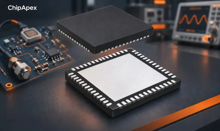
Learn how an analog front end conditions sensor signals. Compare gain, noise, filtering, ADC settling and integration options before selecting components.
Read MoreSN74HCT165PWR is listed in the Shift Registers range at ChipApex. The manufacturer field lists Texas Instruments. Its product description is 8-BIT PARALLEL-IN/SERIAL-OUT SHI. Review…
Read More
SN74HCT165PWR is listed in the Shift Registers range at ChipApex. The manufacturer field lists Texas Instruments. Its product description is 8-BIT PARALLEL-IN/SERIAL-OUT SHI. Review…
Read More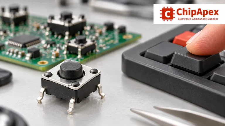
Understand tactile switches, PCB and keyboard differences, four-pin wiring, debounce, force, travel and replacement checks for reliable control inputs.
Read More
The activity of extra discounts on wholesale prices is in full swing…
Please fill in your contact information and we will send you the latest wholesale price list.





