 ChipApex | Global Electronic Components Supplier

SEARCH
Search Product
Search Post
— IC芯片 | 连接器 | 传感器 | 被动器件 —
Search productSearch post
— IC芯片 | 连接器 | 传感器 | 被动器件 —
Consult the customer manager about the wholesale price.
consultation hotline:86-132-6715-2157
email:[email protected]
Contact the product manager for consultation. One-stop consultation is available.
Do you want a lower wholesale price? Please send us your inquiry and we will reply immediately.
2N5115E3 is listed in the Jfets range at ChipApex. The manufacturer field lists Microchip Technology. Its product description is JFET P-CH 30V TO18. Review the specifications below when checking this part for your BOM.
The 2N5115E3 is a P-channel silicon small-signal Junction Field-Effect Transistor (JFET) manufactured by Microchip Technology. It is designed for low-noise and high-reliability applications, featuring a hermetically sealed metal can construction. Key electrical parameters include a drain-source breakdown voltage of 30 V, a gate-source breakdown voltage of 30 V, and a gate-source cutoff voltage of 6 V. The device operates with a zero-bias drain-source current of 7 mA and has a maximum power dissipation of 500 mW. It supports an operating temperature range from -65°C to +200°C.
Verify the specific suffix E3 indicates lead-free compliance against the manufacturer's official datasheet. Confirm that the TO-18 package dimensions match the design requirements. Ensure the ordering quantity meets the manufacturer's minimum order specifications. Check for any military screening options if higher reliability is required for the application.
Select this component when a hermetically sealed P-channel JFET is required for high-temperature operation. Compare the 30 V breakdown voltage and 7 mA IDSS against circuit biasing needs. Consider the TO-18 package constraints for PCB layout or chassis mounting. Verify thermal management capabilities given the 500 mW power dissipation limit.
The 2N5115E3 belongs to the standard 2N5115 series of P-channel JFETs. It serves as the lead-free compliant variant of the traditional 2N5115 device. This series is commonly used in military and aerospace electronics where reliability and radiation hardness are critical. It complements other N-channel variants like the 2N5457 in complementary designs.
Direct pin-compatible replacements include the standard 2N5115 (non-E3) for non-lead-free applications. Other compatible JFETs may require circuit re-biasing due to parameter variations. Verify that substitute devices meet the same high-temperature rating and hermetic sealing requirements.
Explore related parts through Transistors, Discrete Semiconductor Products, all product categories, ChipApex homepage.
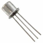 2N5115E3
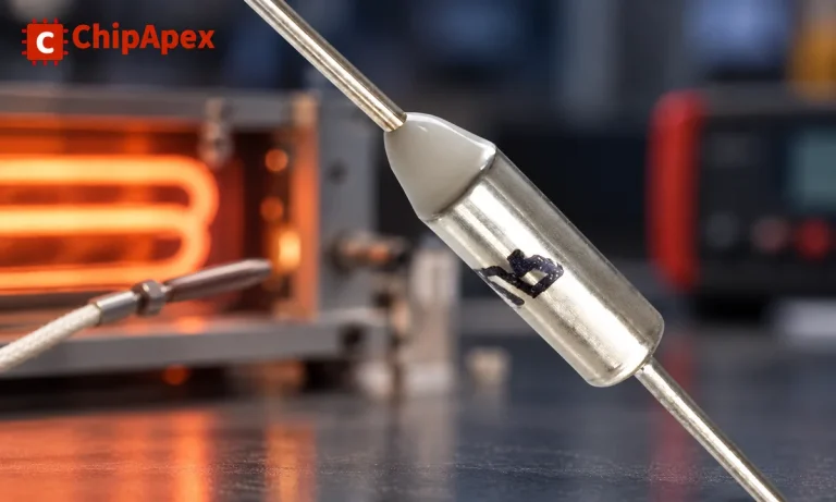
Understand thermal fuse operation, Tf, Th and Tm, electrical ratings and mounting. Check temperature limits and replacement requirements for your design.
Read More
2N5115E3 is listed in the Jfets range at ChipApex. The manufacturer field lists Microchip Technology. Its product description is JFET P-CH 30V TO18. Review…
Read More
Find out when a bare shock switch needs a pull resistor, when an MCU internal pull-up is enough, and why sensor modules and piezo…
Read More
Learn what an IMU measures, how accelerometers and gyroscopes work together, why orientation estimates drift, and what to compare.
Read More
Choose a DIP switch by contact type, coded positions, footprint and signal ratings. Check logic polarity, assembly conditions and PCB configuration behavior.
Read More
2N5115E3 is listed in the Jfets range at ChipApex. The manufacturer field lists Microchip Technology. Its product description is JFET P-CH 30V TO18. Review…
Read More
Learn how a pressure transducer converts pressure into voltage, current, or digital output, and compare pressure references and key selection specs.
Read More
Compare RC, crystal and MEMS oscillator circuits. Check ppm, jitter, load capacitance, startup margin and output compatibility before choosing a clock source.
Read More
2N5115E3 is listed in the Jfets range at ChipApex. The manufacturer field lists Microchip Technology. Its product description is JFET P-CH 30V TO18. Review…
Read More
Choose logic inverter ICs by thresholds, supply, output drive and delay. Compare standard and Schmitt-trigger inputs, power sequencing and replacement checks.
Read More2N5115E3 is listed in the Jfets range at ChipApex. The manufacturer field lists Microchip Technology. Its product description is JFET P-CH 30V TO18. Review…
Read More
2N5115E3 is listed in the Jfets range at ChipApex. The manufacturer field lists Microchip Technology. Its product description is JFET P-CH 30V TO18. Review…
Read More
The activity of extra discounts on wholesale prices is in full swing…
Please fill in your contact information and we will send you the latest wholesale price list.





