 ChipApex | Global Electronic Components Supplier
5SGXMA5N1F45C1G
Search Product
Search Post
— IC芯片 | 连接器 | 传感器 | 被动器件 —
Search productSearch post
— IC芯片 | 连接器 | 传感器 | 被动器件 —
Consult the customer manager about the wholesale price.
consultation hotline:86-132-6715-2157
email:[email protected]
Contact the product manager for consultation. One-stop consultation is available.
Do you want a lower wholesale price? Please send us your inquiry and we will reply immediately.
The Altera 5SGXMA5N1F45C1G is a Stratix V GX Field Programmable Gate Array (FPGA) designed for high-performance digital signal processing and communication applications. It features 490,000 logic elements organized into 185,000 Adaptive Logic Modules (ALMs) and 18,500 Logic Array Blocks (LABs). The device includes 37 Mbit of embedded memory and supports data rates up to 14.1 Gb/s via its transceivers. It operates with a supply voltage range of 0.87V to 0.93V and is housed in a 1932-pin FCBGA package suitable for surface mount installation.
Verify the specific ordering suffix against official manufacturer documentation to ensure correct temperature grade and package variant. Confirm that the component meets all required environmental standards such as RoHS compliance before integration into production designs. Cross-reference the datasheet revision history for any recent updates to electrical characteristics or pin assignments.
Evaluate the total available logic resources against the design complexity to ensure sufficient headroom for optimization. Check the number of available transceivers to match the required serial interface bandwidth. Verify power consumption estimates against thermal management capabilities of the target system board.
This component belongs to the Stratix V GX family, which targets high-performance computing and communications markets. It represents a generation of FPGAs offering significant improvements in logic density and transceiver speed compared to previous generations. The part is manufactured by Altera, now part of Intel.
The integrated transceivers support data rates up to 14.1 Gb/s.
The device contains 37 Mbit of embedded memory.
The core supply voltage operates within a range of 0.87V to 0.93V.
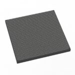 5SGXMA5N1F45C1G
The activity of extra discounts on wholesale prices is in full swing…
Please fill in your contact information and we will send you the latest wholesale price list.






