 ChipApex | Global Electronic Components Supplier
74LVC126ADTR2G
Search Product
Search Post
— IC芯片 | 连接器 | 传感器 | 被动器件 —
Search productSearch post
— IC芯片 | 连接器 | 传感器 | 被动器件 —
Consult the customer manager about the wholesale price.
consultation hotline:86-132-6715-2157
email:[email protected]
Contact the product manager for consultation. One-stop consultation is available.
Do you want a lower wholesale price? Please send us your inquiry and we will reply immediately.
The onsemi 74LVC126ADTR2G is a low-voltage CMOS quad bus buffer featuring non-inverting logic and three-state outputs. It operates within a supply voltage range of 2.0 V to 3.6 V, with a maximum quiescent current of 100 nA. The device utilizes a 14-TSSOP surface-mount package. Propagation delay varies by voltage: 9 ns at 3.3 V and 15 ns at 2.5 V. High-level output current is -8 mA, while low-level output current is 8 mA. It supports an operating temperature range from -55°C to +125°C.
Verify the specific suffix 'ADTR2G' to confirm the TSSOP-14 package and reel packaging configuration. Ensure compatibility with 3.3 V or 2.5 V logic levels. Confirm RoHS compliance status through official manufacturer documentation prior to integration. Cross-reference the part number against the latest datasheet revision to ensure pinout consistency.
Select this component when interfacing between different voltage domains requiring level translation or signal buffering. It is suitable for applications demanding low power dissipation and high noise immunity. Consider the 14-TSSOP footprint for space-constrained designs. Verify that the required drive current does not exceed the specified 8 mA limits under worst-case thermal conditions.
This part belongs to the LVC (Low Voltage CMOS) family, designed for operation below 3.6 V. It serves as a buffer variant within the broader 74-series logic ecosystem. The device complements other LVC components like inverters and gates, providing standardized interface solutions for low-power digital design.
Direct substitutes include MC74LVC126ADTR2G and MC74LCX126ADTR2G, provided voltage levels match. Verify pinout compatibility before swapping. Alternative families may require level shifting adjustments if supply voltages differ significantly.
The maximum supply voltage is 3.6 V.
Yes, the inputs include clamping diodes for transient protection, though external resistors are recommended for voltages exceeding VCC plus one diode drop.
The device is housed in a 14-pin Thin Shrink Small Outline Package (TSSOP).
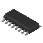 74LVC126ADTR2G
The activity of extra discounts on wholesale prices is in full swing…
Please fill in your contact information and we will send you the latest wholesale price list.





