 ChipApex | Global Electronic Components Supplier
9SQL4958CNDGI
Search Product
Search Post
— IC芯片 | 连接器 | 传感器 | 被动器件 —
Search productSearch post
— IC芯片 | 连接器 | 传感器 | 被动器件 —
Consult the customer manager about the wholesale price.
consultation hotline:86-132-6715-2157
email:[email protected]
Contact the product manager for consultation. One-stop consultation is available.
Do you want a lower wholesale price? Please send us your inquiry and we will reply immediately.
The Renesas 9SQL4958CNDGI is a single-circuit PCI Express clock generator designed for PCIe applications. It operates within a supply voltage range of 3.135V to 3.465V and supports a maximum frequency of 100MHz. The device accepts clock or crystal inputs and provides HCSL and LVCMOS outputs in an 8-output configuration (1:8 ratio). It features a PLL, with differential input/output capability, and is housed in a 48-VFQFN exposed pad package. The component functions reliably across an operating temperature range of -40°C to 85°C.
Verify the specific ordering suffix against official documentation to confirm pinout and electrical characteristics. Confirm RoHS compliance status and moisture sensitivity level prior to procurement. Check for active production status or obsolescence notices from the manufacturer to ensure long-term availability for design-in projects.
Select this component when a dedicated PCIe clock generator with HCSL/LVCMOS outputs is required. Ensure the design accommodates the 3.135V to 3.465V supply voltage range. Verify that the 48-VFQFN footprint matches the PCB layout constraints and thermal requirements for the target operating temperature range.
This part belongs to the Renesas application-specific clock and timing portfolio, focusing on interface standards like PCI Express. It serves as a critical timing source for high-speed serial links, replacing discrete oscillator solutions to save board space and improve signal integrity in complex digital systems.
Consult official substitution guides for direct replacements. Verify compatibility regarding package dimensions, pin assignments, and electrical parameters such as supply voltage and output swing before integrating alternative components into existing designs.
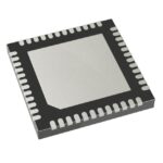 9SQL4958CNDGI
The activity of extra discounts on wholesale prices is in full swing…
Please fill in your contact information and we will send you the latest wholesale price list.






