 ChipApex | Global Electronic Components Supplier

SEARCH
Search Product
Search Post
— IC芯片 | 连接器 | 传感器 | 被动器件 —
Search productSearch post
— IC芯片 | 连接器 | 传感器 | 被动器件 —
Consult the customer manager about the wholesale price.
consultation hotline:86-132-6715-2157
email:[email protected]
Contact the product manager for consultation. One-stop consultation is available.
Do you want a lower wholesale price? Please send us your inquiry and we will reply immediately.
G1NP02LLE is listed in the FET, MOSFET Arrays range at ChipApex. The manufacturer field lists Goford Semiconductor. Its product description is MOSFET 20V 1.3A SOT23-6L. Review the specifications below when checking this part for your BOM.
The G1NP02LLE is a dual-channel enhancement mode power MOSFET from Goford Semiconductor, integrating one N-channel and one P-channel device in an SOT-23-6L package. The NMOS supports a drain-source voltage of 20V with a continuous current of 1.3A at 25°C, while the PMOS handles -20V and -1.1A. Both channels utilize advanced trench technology for low on-resistance and gate charge. Key electrical parameters include an NMOS RDS(on) max of 210mΩ at VGS=4.5V and a PMOS RDS(on) max of 460mΩ at VGS=-4.5V. The component operates within a junction temperature range of -55°C to 150°C.
Verify the specific ordering suffix and packaging configuration against official distributor catalogs before purchase. Confirm that the SOT-23-6L dual package marking matches the required schematic pinout for your design. Ensure compliance with RoHS standards and check for any specific ESD handling requirements during assembly.
Select this component for applications requiring a matched NMOS/PMOS pair in a minimal footprint. The low gate charge facilitates faster switching speeds, reducing dynamic losses in DC/DC converter designs. Verify that the 20V breakdown voltage and current ratings align with the system's maximum operating conditions and thermal dissipation capabilities.
This part belongs to Goford Semiconductor's lineup of dual-channel power MOSFETs designed for space-constrained electronics. It serves as a complementary pair solution, simplifying circuit layouts for half-bridge or synchronous rectification topologies compared to using discrete single-channel devices.
G1NP02E
The maximum continuous drain current (ID) for the NMOS channel is 1.3A at a case temperature of 25°C.
Yes, both the NMOS and PMOS channels are 100% avalanche tested to ensure reliability under transient events.
The typical total gate charge (Qg) for the NMOS is 1nC, measured at VDD=10V, ID=0.65A, and VGS=4.5V.
Explore related parts through FETs, MOSFETs, Transistors, Discrete Semiconductor Products, all product categories.
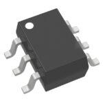 G1NP02LLE

G1NP02LLE is listed in the FET, MOSFET Arrays range at ChipApex. The manufacturer field lists Goford Semiconductor. Its product description is MOSFET 20V 1.3A…
Read More
G1NP02LLE is listed in the FET, MOSFET Arrays range at ChipApex. The manufacturer field lists Goford Semiconductor. Its product description is MOSFET 20V 1.3A…
Read More
G1NP02LLE is listed in the FET, MOSFET Arrays range at ChipApex. The manufacturer field lists Goford Semiconductor. Its product description is MOSFET 20V 1.3A…
Read More
G1NP02LLE is listed in the FET, MOSFET Arrays range at ChipApex. The manufacturer field lists Goford Semiconductor. Its product description is MOSFET 20V 1.3A…
Read More
Compare Pt100 and Pt1000 RTDs, two-, three- and four-wire connections, excitation and self-heating. Build an error budget from element to reported temperature.
Read More
G1NP02LLE is listed in the FET, MOSFET Arrays range at ChipApex. The manufacturer field lists Goford Semiconductor. Its product description is MOSFET 20V 1.3A…
Read More
G1NP02LLE is listed in the FET, MOSFET Arrays range at ChipApex. The manufacturer field lists Goford Semiconductor. Its product description is MOSFET 20V 1.3A…
Read More
Compare RC, crystal and MEMS oscillator circuits. Check ppm, jitter, load capacitance, startup margin and output compatibility before choosing a clock source.
Read More
G1NP02LLE is listed in the FET, MOSFET Arrays range at ChipApex. The manufacturer field lists Goford Semiconductor. Its product description is MOSFET 20V 1.3A…
Read More
Learn why PTC resistance rises with temperature, how it differs from NTC, and which ratings matter for sensing and protection.
Read More
G1NP02LLE is listed in the FET, MOSFET Arrays range at ChipApex. The manufacturer field lists Goford Semiconductor. Its product description is MOSFET 20V 1.3A…
Read More
G1NP02LLE is listed in the FET, MOSFET Arrays range at ChipApex. The manufacturer field lists Goford Semiconductor. Its product description is MOSFET 20V 1.3A…
Read More
The activity of extra discounts on wholesale prices is in full swing…
Please fill in your contact information and we will send you the latest wholesale price list.





