 ChipApex | Global Electronic Components Supplier

SEARCH
Search Product
Search Post
— IC芯片 | 连接器 | 传感器 | 被动器件 —
Search productSearch post
— IC芯片 | 连接器 | 传感器 | 被动器件 —
Consult the customer manager about the wholesale price.
consultation hotline:86-132-6715-2157
email:[email protected]
Contact the product manager for consultation. One-stop consultation is available.
Do you want a lower wholesale price? Please send us your inquiry and we will reply immediately.
LFE3-150EA-8LFN672C is listed in the Field Programmable Gate Array range at ChipApex. The manufacturer field lists Lattice Semiconductor Corporation. Its product description is IC FPGA 380 I/O 672FPBGA. Review the specifications below when checking this part for your BOM.
The LFE3-150EA-8LFN672C is a Field Programmable Gate Array from the Lattice ECP3 family, manufactured by Lattice Semiconductor Corporation. It features 149,000 logic elements and 74,500 Adaptive Logic Modules within an industrial temperature range of -40°C to +100°C. The device includes 6.69 Mbit of embedded memory and supports up to 380 I/Os. Operating at a minimum voltage of 1.14 V and maximum of 1.26 V, it utilizes a 672-pin FPBGA package for surface mount installation. The component supports data rates up to 3.2 Gb/s and is designed for high-volume, cost-effective applications requiring high-speed interfaces.
Verify the specific speed grade suffix against official Lattice documentation to ensure compatibility with timing requirements. Confirm that the 8LFN672C designation aligns with the intended thermal and electrical specifications for the target application environment before finalizing procurement orders.
Select this model when designing systems requiring 149K logic elements and extensive memory resources within a 672-pin footprint. Ensure the design accommodates the 1.2V core voltage requirements and verify that the FPBGA-672 package dimensions fit the PCB layout constraints effectively.
This component belongs to the Lattice ECP3 FPGA family, which targets high-volume, low-cost applications. The series expands look-up-table capacity significantly compared to previous generations, offering enhanced DSP architectures and high-speed I/O capabilities suitable for edge computing and connectivity solutions.
Consult official Lattice cross-reference guides for verified substitutes. Consider the LFE3-150EA-6LFN672C or LFE3-150EA-7LFN672C if lower speed grades are acceptable, ensuring pinout and functional compatibility remain unchanged.
Explore related parts through Embedded, Integrated Circuits (ICs), all product categories, ChipApex homepage.
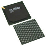 LFE3-150EA-8LFN672C
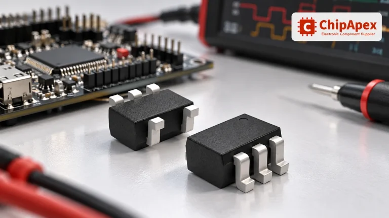
Choose logic inverter ICs by thresholds, supply, output drive and delay. Compare standard and Schmitt-trigger inputs, power sequencing and replacement checks.
Read More
LFE3-150EA-8LFN672C is listed in the Field Programmable Gate Array range at ChipApex. The manufacturer field lists Lattice Semiconductor Corporation. Its product description is IC…
Read More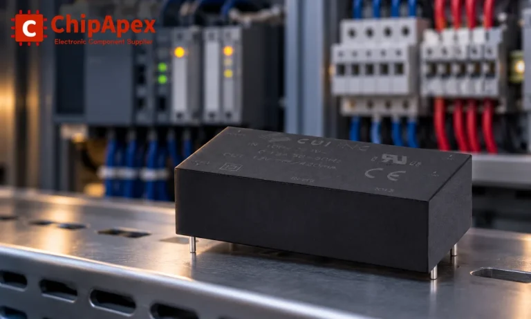
Choose an AC to DC converter by input range, output demand, isolation, efficiency and thermal derating. Compare architectures and check installation needs.
Read More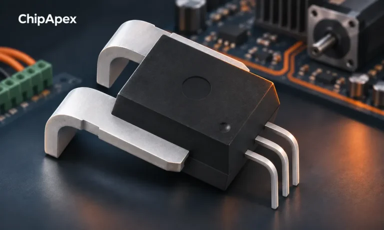
Compare Hall, shunt, current transformer and Rogowski sensing. Check AC/DC capability, accuracy, isolation, heat and response before selecting a sensor.
Read More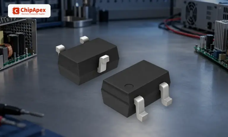
Learn how a diode conducts, how to identify anode and cathode, and when to choose rectifier, TVS, Zener or photodiode types for a circuit.
Read More
LFE3-150EA-8LFN672C is listed in the Field Programmable Gate Array range at ChipApex. The manufacturer field lists Lattice Semiconductor Corporation. Its product description is IC…
Read More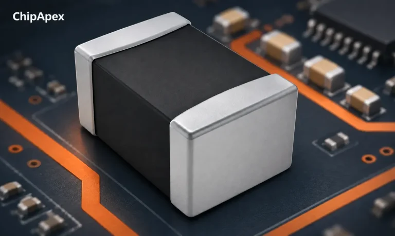
Learn how to use ferrite beads for noise filtering. Check impedance, DC bias, placement, resonance and load-step behavior before selecting a part.
Read More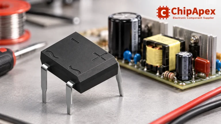
Select a bridge rectifier by reverse voltage, capacitor charging current, startup surge and cooling. Work through a stated DC voltage and ripple example.
Read More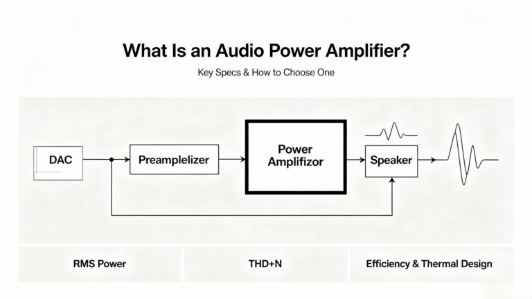
LFE3-150EA-8LFN672C is listed in the Field Programmable Gate Array range at ChipApex. The manufacturer field lists Lattice Semiconductor Corporation. Its product description is IC…
Read More
LFE3-150EA-8LFN672C is listed in the Field Programmable Gate Array range at ChipApex. The manufacturer field lists Lattice Semiconductor Corporation. Its product description is IC…
Read More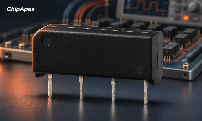
Choose a reed relay for signal switching. Understand hot and cold switching, leakage, contact resistance, isolation and measurement settling requirements.
Read More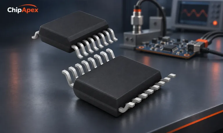
Choose an ADC converter by resolution, sample rate, noise and input design. Review practical tradeoffs and prepare component requirements for ChipApex.
Read More
The activity of extra discounts on wholesale prices is in full swing…
Please fill in your contact information and we will send you the latest wholesale price list.





