ChipApex | Global Electronic Components Supplier

SEARCH
Search Product
Search Post
— IC芯片 | 连接器 | 传感器 | 被动器件 —
Search productSearch post
— IC芯片 | 连接器 | 传感器 | 被动器件 —
Consult the customer manager about the wholesale price.
consultation hotline:86-132-6715-2157
email:[email protected]
Contact the product manager for consultation. One-stop consultation is available.
Do you want a lower wholesale price? Please send us your inquiry and we will reply immediately.
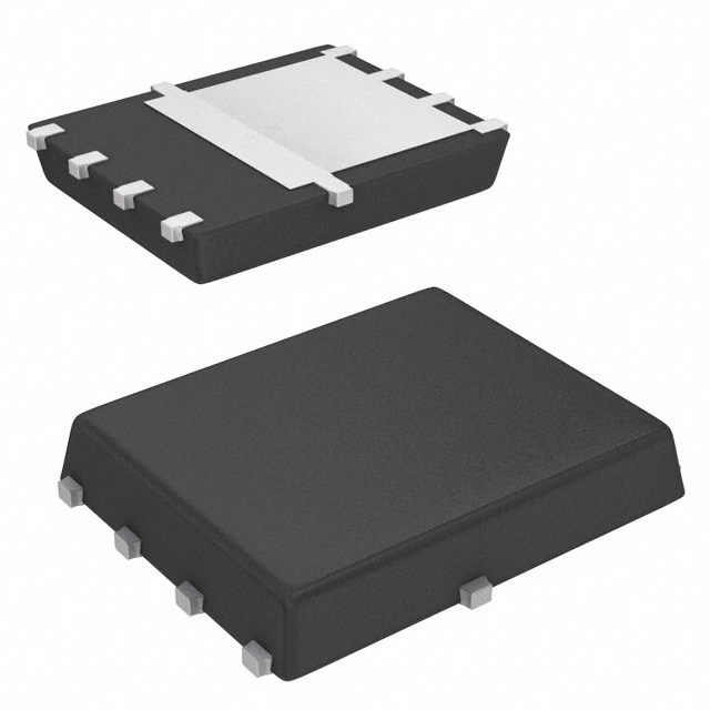
SIR1309DP-T1-GE3 is listed in the Single FETs, MOSFETs range at ChipApex. The manufacturer field lists Vishay Siliconix. Its product description is P-CHANNEL 30 V (D-S) MOSFET POWE. Review the specifications below when checking this part for your BOM.
The Vishay Siliconix SiR1309DP is a P-Channel power MOSFET utilizing TrenchFET Gen IV technology. It features a -30 V drain-source voltage and a maximum on-state resistance of 7.3 mΩ at VGS = -10 V. The device supports a continuous drain current of -65.7 A at TC = 25 °C and dissipates up to 56.8 W under the same conditions. Packaged in a leadless PowerPAK SO-8, it operates within a junction temperature range of -55 °C to +150 °C.
Verify component authenticity by cross-referencing the manufacturer part number with official datasheet documentation. Confirm that the ordering suffix matches the specified lead-free and halogen-free configuration. Ensure all technical parameters align with the required application specifications before finalizing procurement decisions.
Select this component based on its specific -30 V rating and low on-resistance characteristics suitable for high-current applications. Evaluate the thermal requirements against the provided junction-to-case resistance values. Consider the single-channel configuration and PowerPAK SO-8 footprint when designing the printed circuit board layout.
This component belongs to the Vishay Siliconix TrenchFET family, designed for general-purpose power switching applications. It represents an evolution in silicon-based MOSFET technology, focusing on reducing conduction losses while maintaining robust reliability standards across various industrial and consumer electronic environments.
Consult official Vishay documentation for verified substitute part numbers. Do not assume compatibility with other manufacturers' devices without validating pinout, electrical ratings, and thermal characteristics against the original specifications.
The absolute maximum gate-source voltage rating is ±25 V.
Yes, the datasheet confirms that 100% of the units are tested for unclamped inductive switching (UIS).
Explore related parts through FETs, MOSFETs, Transistors, Discrete Semiconductor Products, all product categories.
 SIR1309DP-T1-GE3

Select MOV varistors by continuous voltage, clamping behavior, surge waveform and repetition. Check thermal disconnection, fuse coordination and replacements.
Read More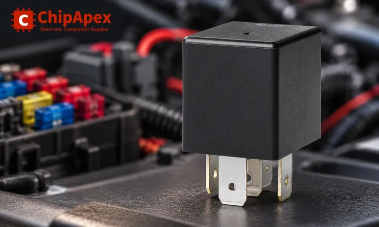
Learn the relay definition, coil and contact operation, NO and NC forms, load ratings and suppression choices. Compare mechanical, reed and solid-state types.
Read More
Compare RC, crystal and MEMS oscillator circuits. Check ppm, jitter, load capacitance, startup margin and output compatibility before choosing a clock source.
Read More
SIR1309DP-T1-GE3 is listed in the Single FETs, MOSFETs range at ChipApex. The manufacturer field lists Vishay Siliconix. Its product description is P-CHANNEL 30 V…
Read More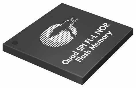
SIR1309DP-T1-GE3 is listed in the Single FETs, MOSFETs range at ChipApex. The manufacturer field lists Vishay Siliconix. Its product description is P-CHANNEL 30 V…
Read More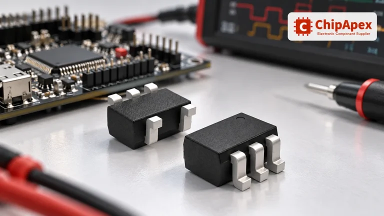
Choose logic inverter ICs by thresholds, supply, output drive and delay. Compare standard and Schmitt-trigger inputs, power sequencing and replacement checks.
Read More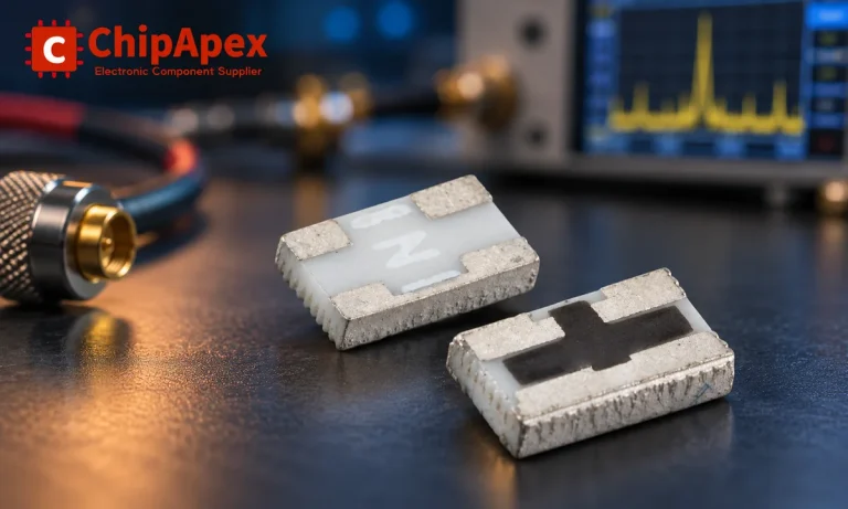
Understand RF attenuator dB values, fixed and programmable types, impedance, power limits and noise tradeoffs before choosing parts for an RF signal path.
Read More
SIR1309DP-T1-GE3 is listed in the Single FETs, MOSFETs range at ChipApex. The manufacturer field lists Vishay Siliconix. Its product description is P-CHANNEL 30 V…
Read More
SIR1309DP-T1-GE3 is listed in the Single FETs, MOSFETs range at ChipApex. The manufacturer field lists Vishay Siliconix. Its product description is P-CHANNEL 30 V…
Read More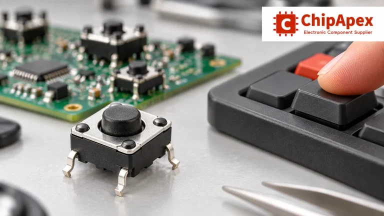
Choose tactile switches by operating force, travel, actuator height, footprint and lifetime. Check debounce, sealing and the assembled button mechanism.
Read More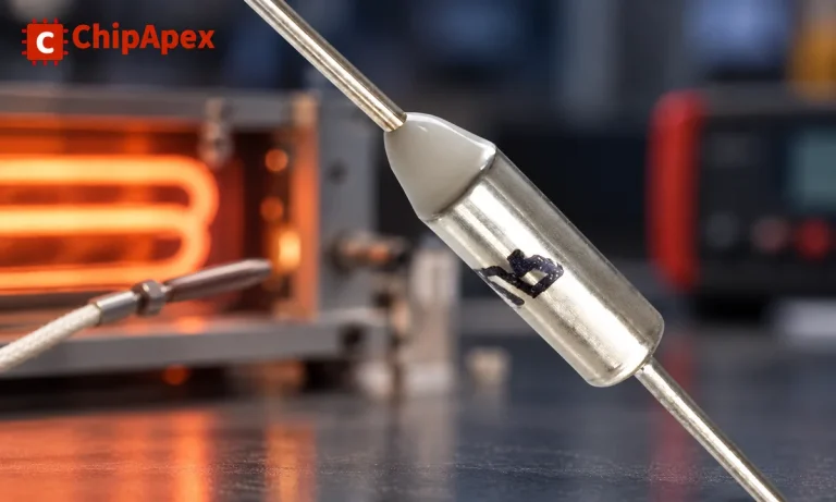
Understand thermal fuse operation, Tf, Th and Tm, electrical ratings and mounting. Check temperature limits and replacement requirements for your design.
Read More
Find out when a bare shock switch needs a pull resistor, when an MCU internal pull-up is enough, and why sensor modules and piezo…
Read More
The activity of extra discounts on wholesale prices is in full swing…
Please fill in your contact information and we will send you the latest wholesale price list.