 ChipApex | Global Electronic Components Supplier

SEARCH
Search Product
Search Post
— IC芯片 | 连接器 | 传感器 | 被动器件 —
Search productSearch post
— IC芯片 | 连接器 | 传感器 | 被动器件 —
Consult the customer manager about the wholesale price.
consultation hotline:86-132-6715-2157
email:[email protected]
Contact the product manager for consultation. One-stop consultation is available.
Do you want a lower wholesale price? Please send us your inquiry and we will reply immediately.
SY898535LKY is listed in the Clock Buffers, Drivers range at ChipApex. The manufacturer field lists Microchip Technology. Its product description is IC CLK BUFFER 2:4 235MHZ 20TSSOP. Review the specifications below when checking this part for your BOM.
The SY898535LKY is a Precision Edge low skew fanout buffer manufactured by Microchip Technology. It translates single-ended LVCMOS or LVTTL inputs to four differential 3.3V LVPECL outputs. The device features two selectable clock inputs (CLK0, CLK1) and a synchronous clock enable pin. Operating from a 3.3V ±5% supply, it supports maximum output frequencies up to 235MHz with propagation delays under 1.9ns and output skew below 30ps. Additive phase jitter is typically 0.09ps RMS. It operates within an industrial temperature range of –40°C to +85°C and is housed in a 20-pin TSSOP package.
Verify the specific ordering suffix against official documentation to confirm packaging details. The 'K' suffix indicates the 20-pin TSSOP package type, while 'Y' denotes the industrial temperature operating range. Confirm whether the required unit quantity corresponds to tape and reel specifications if applicable.
Select this component when interfacing LVCMOS or LVTTL sources to LVPECL loads requiring low skew distribution. Ensure the design accommodates a 3.3V ±5% power supply and operates within the specified -40°C to +85°C temperature limits. Verify that the 235MHz maximum frequency meets system timing requirements.
The SY898535L belongs to Micrel’s Precision Edge product line, designed for high-speed signal integrity. This specific part number represents the industrial grade variant packaged in a 20-pin TSSOP format. It serves as a bridge between standard logic levels and high-speed differential signaling standards.
Consult official cross-reference lists for verified substitutes. Generic family members may share similar functionality but require verification of electrical parameters and pin compatibility before implementation.
The clock enable pin is synchronized with the input signal to eliminate runt pulses on the outputs during asynchronous assertion or de-assertion.
CLK_EN has an internal 51kΩ pull-up resistor defaulting to HIGH. CLK_SEL has an internal 51kΩ pull-down resistor defaulting to LOW, selecting the CLK0 input.
The differential LVPECL outputs have a typical peak-to-peak voltage swing of 800mV.
Explore related parts through Clock/Timing, Integrated Circuits (ICs), all product categories, ChipApex homepage.
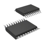 SY898535LKY
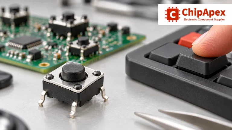
Choose tactile switches by operating force, travel, actuator height, footprint and lifetime. Check debounce, sealing and the assembled button mechanism.
Read More
SY898535LKY is listed in the Clock Buffers, Drivers range at ChipApex. The manufacturer field lists Microchip Technology. Its product description is IC CLK BUFFER…
Read More
Find out when a bare shock switch needs a pull resistor, when an MCU internal pull-up is enough, and why sensor modules and piezo…
Read More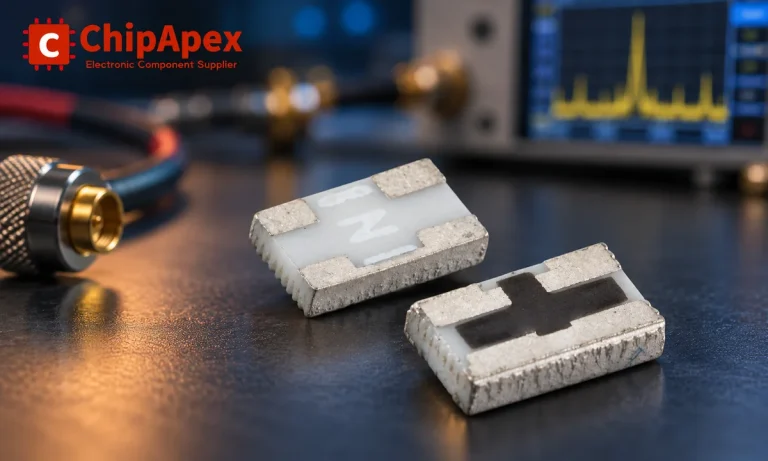
Understand RF attenuator dB values, fixed and programmable types, impedance, power limits and noise tradeoffs before choosing parts for an RF signal path.
Read More
SY898535LKY is listed in the Clock Buffers, Drivers range at ChipApex. The manufacturer field lists Microchip Technology. Its product description is IC CLK BUFFER…
Read More
Choose a DIP switch by contact type, coded positions, footprint and signal ratings. Check logic polarity, assembly conditions and PCB configuration behavior.
Read More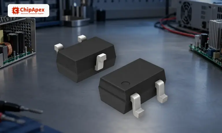
Learn how a diode conducts, how to identify anode and cathode, and when to choose rectifier, TVS, Zener or photodiode types for a circuit.
Read More
SY898535LKY is listed in the Clock Buffers, Drivers range at ChipApex. The manufacturer field lists Microchip Technology. Its product description is IC CLK BUFFER…
Read More
Select MOV varistors by continuous voltage, clamping behavior, surge waveform and repetition. Check thermal disconnection, fuse coordination and replacements.
Read More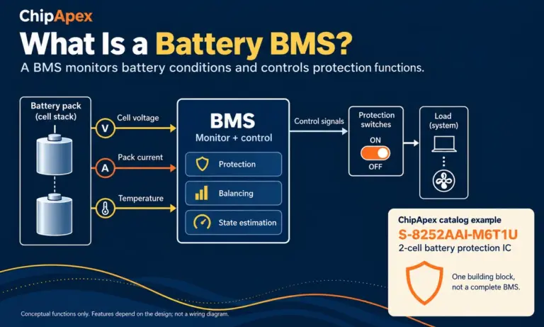
Learn what a battery BMS does, how protection differs from charging, and which pack specifications to check when sourcing BMS components through ChipApex.
Read More
SY898535LKY is listed in the Clock Buffers, Drivers range at ChipApex. The manufacturer field lists Microchip Technology. Its product description is IC CLK BUFFER…
Read More
See how a MEMS gyroscope measures angular rate, why its angle estimate drifts, and which range, noise, interface and temperature specs to compare.
Read More
The activity of extra discounts on wholesale prices is in full swing…
Please fill in your contact information and we will send you the latest wholesale price list.






