 ChipApex | Global Electronic Components Supplier

SEARCH
Search Product
Search Post
— IC芯片 | 连接器 | 传感器 | 被动器件 —
Search productSearch post
— IC芯片 | 连接器 | 传感器 | 被动器件 —
Consult the customer manager about the wholesale price.
consultation hotline:86-132-6715-2157
email:[email protected]
Contact the product manager for consultation. One-stop consultation is available.
Do you want a lower wholesale price? Please send us your inquiry and we will reply immediately.
A3I25X050NR1 is listed in the RF FETs, MOSFETs range at ChipApex. The manufacturer field lists NXP USA Inc.. Its product description is RF MOSFET LDMOS 28V OM400-8. Review the specifications below when checking this part for your BOM.
The A3I25X050NR1 is an Airfast RF LDMOS integrated power amplifier designed for operation from 2300 to 2700 MHz. It features a multi-stage Doherty circuit with on-chip matching, supporting 20 to 32 Vdc drain voltage. Typical performance at 28 Vdc includes 5.6 W average output power with 39.5% PAE and -35.6 dBc ACPR, or 8.7 W average output power with 44.8% PAE and -31.9 dBc ACPR at 2590 MHz using single-carrier W-CDMA signals.
Verify the specific ordering suffix against official documentation to confirm package type and reel specifications. The R1 suffix indicates tape and reel packaging with defined unit counts and tape width. Confirm RoHS compliance status and ensure compatibility with required thermal management solutions for the specified operating junction temperature range.
Select this component for designs requiring integrated Doherty functionality within the 2300–2700 MHz band. Ensure the application supports the required gate bias voltages for carrier and peaking stages. Validate thermal resistance characteristics against system heat dissipation capabilities. Verify that the input signal parameters align with the characterization test conditions for optimal linearity and efficiency.
This device belongs to NXP's Airfast RF LDMOS integrated power amplifier family. It utilizes advanced laterally diffused MOS technology to combine high power density with integrated matching networks. The design targets modern cellular base stations requiring efficient amplification of complex modulation schemes across wide frequency bands.
Consult official NXP documentation for verified substitute part numbers. Cross-referencing requires matching electrical specifications, pin configurations, and thermal characteristics. Do not assume interchangeability without validating functional equivalence through manufacturer-approved resources.
The maximum operating junction temperature is +225 °C.
The exposed backside of the package serves as the source terminal for the transistor.
The device meets Human Body Model Class 1C and Charge Device Model Class C3 per specified testing methodologies.
Explore related parts through FETs, MOSFETs, Transistors, Discrete Semiconductor Products, all product categories.
 A3I25X050NR1

Compare Pt100 and Pt1000 RTDs, two-, three- and four-wire connections, excitation and self-heating. Build an error budget from element to reported temperature.
Read More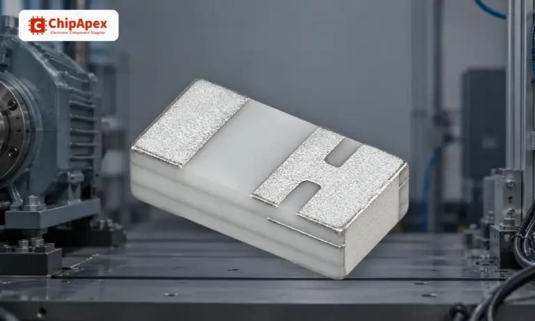
Find out when a bare shock switch needs a pull resistor, when an MCU internal pull-up is enough, and why sensor modules and piezo…
Read More
A3I25X050NR1 is listed in the RF FETs, MOSFETs range at ChipApex. The manufacturer field lists NXP USA Inc.. Its product description is RF MOSFET…
Read More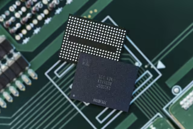
A3I25X050NR1 is listed in the RF FETs, MOSFETs range at ChipApex. The manufacturer field lists NXP USA Inc.. Its product description is RF MOSFET…
Read More
A3I25X050NR1 is listed in the RF FETs, MOSFETs range at ChipApex. The manufacturer field lists NXP USA Inc.. Its product description is RF MOSFET…
Read More
A3I25X050NR1 is listed in the RF FETs, MOSFETs range at ChipApex. The manufacturer field lists NXP USA Inc.. Its product description is RF MOSFET…
Read More
A3I25X050NR1 is listed in the RF FETs, MOSFETs range at ChipApex. The manufacturer field lists NXP USA Inc.. Its product description is RF MOSFET…
Read More
Choose an AC to DC converter by input range, output demand, isolation, efficiency and thermal derating. Compare architectures and check installation needs.
Read More
A3I25X050NR1 is listed in the RF FETs, MOSFETs range at ChipApex. The manufacturer field lists NXP USA Inc.. Its product description is RF MOSFET…
Read More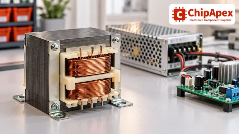
Select power transformers by input frequency, secondary VA, rectifier load, isolation, regulation and inrush. Build a clearer specification for your next RFQ.
Read More
Select MOV varistors by continuous voltage, clamping behavior, surge waveform and repetition. Check thermal disconnection, fuse coordination and replacements.
Read More
A3I25X050NR1 is listed in the RF FETs, MOSFETs range at ChipApex. The manufacturer field lists NXP USA Inc.. Its product description is RF MOSFET…
Read More
The activity of extra discounts on wholesale prices is in full swing…
Please fill in your contact information and we will send you the latest wholesale price list.





